欧洲半导体计量和检测市场预测至 2028 年 – COVID-19 影响和区域分析 – 按类型(晶圆检测系统、掩模检测系统和薄膜计量)、技术(光学和电子束)和组织规模(大型企业和中小企业)
No. of Pages: 125 | Report Code: BMIRE00027261 | Category: Electronics and Semiconductor
No. of Pages: 125 | Report Code: BMIRE00027261 | Category: Electronics and Semiconductor
欧洲半导体计量和检测市场
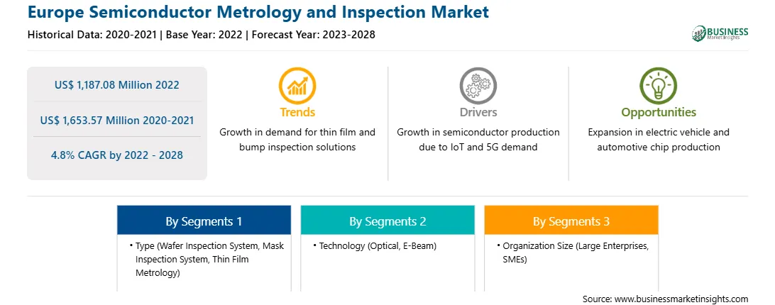
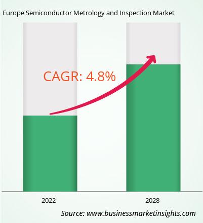
预计将从 2022 年的 1,187.08 亿美元增长到 1,653.57 美元<到 2028 年将达到 100 万;预计 2022 年至 2028 年复合年增长率为 4.8%。
晶圆制造、制造、等工序均采用先进封装(AP)技术。在后端控制这些操作需要检查和测量方法。不断缩小的特征尺寸推动了对高精度、精密度、灵敏度和吞吐量的需求。另一方面,AP 程序面临后端应用特有的测量和检查问题,例如凸点测量和非视觉缺陷。特殊要求,加上 AP 工艺的多样性和快速发展,推动了对灵活测量和检测系统的需求,这些系统可以控制各种参数,包括二维 (2D) 和三维 (3D) 几何形状,以及可以适应出现的新要求。将各种能力整合到一个平台中是最经济、最有效的资本利用方式。跟上行业发展路线图需要设备提供商提供新颖的解决方案,重点关注 AP 运营的独特要求。例如,KLA Corporation 在 3D IC 和高密度扇出等先进晶圆级封装 (AWLP) 应用中提供具有高分辨率光学器件的 Kronos 1190 图案化晶圆检测系统。该系统使流程开发和生产监控的重要缺陷变得敏感。制造商面临着提高质量和可靠性的压力。在汽车等行业尤其如此,消费者安全是这些行业的主要关注点。汽车中存在数以千计的半导体元件。此外,完全无人驾驶的车辆的组件数量可能会增加几个数量级。对于一辆拥有一万个零部件的汽车来说,百万分之一的零部件故障率相当于百分之一的整车故障率,这是不可接受的。为了应对当前和下一代封装中的这一挑战,需要低至微米级的缺陷灵敏度,以及在大量原始数据流中快速、一致地识别致命故障的能力。仪表重复性和再现性 (R&R) 研究变得越来越重要。工程师需要技术将原始数据转化为有用的过程知识。电子束技术也被应用于先进封装中。电子在电子束检查系统的工具内产生,然后撞击模具的表面。电子散射并反弹回检测器,使其能够检测有故障的芯片。
借助新功能和技术,供应商可以吸引新客户并扩大其在新兴市场的足迹。这一因素可能会推动欧洲半导体计量和检测市场。 欧洲半导体计量和检测市场预计在预测期内将以良好的复合年增长率增长。
到 2028 年欧洲半导体计量和检测市场收入及预测(百万美元)
< strong>
欧洲半导体计量检测市场细分
欧洲半导体计量和检测市场细分基于类型、技术、组织规模和国家/地区。根据类型,欧洲半导体计量和检测市场分为晶圆检测系统、掩模检测系统和薄膜计量。晶圆检测系统领域在 2022 年占据市场主导地位。根据技术,欧洲半导体计量和检测市场分为光学和电子束。到2022年,光学领域将主导市场。根据组织规模,欧洲半导体计量和检测市场分为大型企业和中小企业。大型企业细分市场将在 2022 年占据主导地位。根据国家/地区,欧洲半导体计量和检测市场已细分为英国、德国、法国、意大利、俄罗斯和欧洲其他地区。德国将在 2022 年占据市场主导地位。
应用材料公司;阿斯麦控股公司;日立高新技术公司;日本电子有限公司; KLA 公司;激光技术公司;尼康计量公司;诺瓦有限公司;创新;和 Thermo Fisher Scientific Inc. 是欧洲半导体计量和检测市场的领先公司之一。
Strategic insights for Europe Semiconductor Metrology and Inspection involve closely monitoring industry trends, consumer behaviours, and competitor actions to identify opportunities for growth. By leveraging data analytics, businesses can anticipate market shifts and make informed decisions that align with evolving customer needs. Understanding these dynamics helps companies adjust their strategies proactively, enhance customer engagement, and strengthen their competitive edge. Building strong relationships with stakeholders and staying agile in response to changes ensures long-term success in any market.
| Report Attribute | Details |
|---|---|
| Market size in 2022 | US$ 1,187.08 Million |
| Market Size by 2028 | US$ 1,653.57 Million |
| Global CAGR (2022 - 2028) | 4.8% |
| Historical Data | 2020-2021 |
| Forecast period | 2023-2028 |
| Segments Covered |
By 类型
|
| Regions and Countries Covered | 欧洲
|
| Market leaders and key company profiles |
The regional scope of Europe Semiconductor Metrology and Inspection refers to the geographical area in which a business operates and competes. Understanding regional nuances, such as local consumer preferences, economic conditions, and regulatory environments, is crucial for tailoring strategies to specific markets. Businesses can expand their reach by identifying underserved regions or adapting their offerings to meet regional demands. A clear regional focus allows for more effective resource allocation, targeted marketing, and better positioning against local competitors, ultimately driving growth in those specific areas.
The Europe Semiconductor Metrology and Inspection Market is valued at US$ 1,187.08 Million in 2022, it is projected to reach US$ 1,653.57 Million by 2028.
As per our report Europe Semiconductor Metrology and Inspection Market, the market size is valued at US$ 1,187.08 Million in 2022, projecting it to reach US$ 1,653.57 Million by 2028. This translates to a CAGR of approximately 4.8% during the forecast period.
The Europe Semiconductor Metrology and Inspection Market report typically cover these key segments-
The historic period, base year, and forecast period can vary slightly depending on the specific market research report. However, for the Europe Semiconductor Metrology and Inspection Market report:
The Europe Semiconductor Metrology and Inspection Market is populated by several key players, each contributing to its growth and innovation. Some of the major players include:
The Europe Semiconductor Metrology and Inspection Market report is valuable for diverse stakeholders, including:
Essentially, anyone involved in or considering involvement in the Europe Semiconductor Metrology and Inspection Market value chain can benefit from the information contained in a comprehensive market report.
Office No. 1011, First floor, Farena Corporate Park, Magarpatta-Mundhwa road, Pune - 411028, Maharashtra, India
US:+16467917070
sales@businessmarketinsights.com


 Get Free Sample For Europe Semiconductor Metrology and Inspection Market
