亚太地区硅 EPI 晶圆市场预测至 2028 年 – COVID-19 影响和区域分析 – 晶圆尺寸(6 英寸、8 英寸、12 英寸等)、应用(LED、功率半导体和基于 MEMS 的器件) )、最终用户(消费电子、汽车、医疗保健、航空航天和国防等)和类型(异质外延和同质外延)
No. of Pages: 143 | Report Code: BMIRE00025998 | Category: Electronics and Semiconductor
No. of Pages: 143 | Report Code: BMIRE00025998 | Category: Electronics and Semiconductor
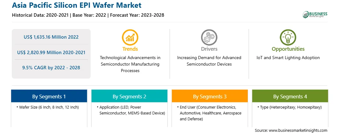
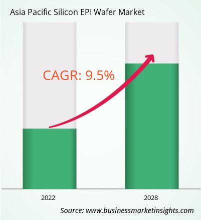
亚太硅EPI晶圆市场预计将从2022年的16.3516亿美元增长到2028年的28.2099亿美元;预计 2022 年至 2028 年复合年增长率为 9.5%。
氮化镓 (GaN)、宽带隙半导体,支持器件在比硅基器件更高的温度和电压下运行。 GaN 更大的介电击穿也使得构建具有更低电阻的更小器件成为可能。电阻越低,器件越小,电容(导通)越小。外延GaN晶片具有高效率和高功率输出的特点,是用于功率和射频(RF)器件的基础材料。它们用于国防雷达、电动汽车电源转换器、5G 基站和 IT 设备快速充电器。例如,韩国IVWorks利用基于深度学习的人工智能(AI)外延技术,使氮化镓外延片成为直流功率器件和5G通信设备的关键组件,进一步吸引了670万美元的B轮投资。由于其高电子迁移率、电流密度和击穿电压,GaN 可用于制造在高频下工作的高效、高输出功率器件。它比 Si、SiC 和 GaAs 材料更小、更快、更高效,并且比这些材料产生更多的电力。与 Si、SiC 和 GaAs(Si 或 SiC)不同,GaN 在独立式晶圆技术方面尚未得到充分开发,因此在异质衬底上需要进行 GaN 外延生长。尽管 Si 可以经济地处理大直径晶圆,但由于与 GaN 存在巨大的晶格失配和热膨胀系数差异,因此需要一种管理应力和缺陷密度的技术。基于人工智能的 GaN 晶圆的不断进步为硅 EPI 晶圆市场的未来增长提供了利润丰厚的机会。
亚洲供应商-太平洋硅EPI晶圆市场可以通过提供创新产品吸引新客户并扩大其在新兴市场的足迹。这可能会在预测期内推动市场实现显着的复合年增长率。
亚太硅业EPI晶圆市场细分
亚太地区;硅 EPI 晶圆市场根据晶圆尺寸、应用、最终用户、类型和国家进行细分。根据晶圆尺寸,市场分为6英寸、8英寸、12英寸等。根据应用,市场分为 LED、功率半导体和基于 MEMS 的器件。按最终用户划分,亚太地区硅 EPI 晶圆市场分为消费电子、汽车、医疗保健、航空航天和国防等。根据类型,市场分为异质外延和同质外延。按国家/地区划分,亚太地区硅 EPI 晶圆市场分为台湾、中国、印度、日本、韩国和亚太地区其他地区。
亚太硅外延硅片市场—— 提及的公司
Applied Materials, Inc.; II-VI 公司;信越化学有限公司;森科公司;世创电子股份公司;日亚化学工业株式会社;环球晶圆日本有限公司; EpiGaN nv(Soitec 比利时 NV)和 SK Siltron Co., Ltd 是亚太硅 EPI 晶圆市场的主要运营公司之一。
Strategic insights for Asia Pacific Silicon EPI Wafer involve closely monitoring industry trends, consumer behaviours, and competitor actions to identify opportunities for growth. By leveraging data analytics, businesses can anticipate market shifts and make informed decisions that align with evolving customer needs. Understanding these dynamics helps companies adjust their strategies proactively, enhance customer engagement, and strengthen their competitive edge. Building strong relationships with stakeholders and staying agile in response to changes ensures long-term success in any market.
| Report Attribute | Details |
|---|---|
| Market size in 2022 | US$ 1,635.16 Million |
| Market Size by 2028 | US$ 2,820.99 Million |
| Global CAGR (2022 - 2028) | 9.5% |
| Historical Data | 2020-2021 |
| Forecast period | 2023-2028 |
| Segments Covered |
By 晶圆尺寸
|
| Regions and Countries Covered | 亚太地区
|
| Market leaders and key company profiles |
The regional scope of Asia Pacific Silicon EPI Wafer refers to the geographical area in which a business operates and competes. Understanding regional nuances, such as local consumer preferences, economic conditions, and regulatory environments, is crucial for tailoring strategies to specific markets. Businesses can expand their reach by identifying underserved regions or adapting their offerings to meet regional demands. A clear regional focus allows for more effective resource allocation, targeted marketing, and better positioning against local competitors, ultimately driving growth in those specific areas.
The Asia Pacific Silicon EPI Wafer Market is valued at US$ 1,635.16 Million in 2022, it is projected to reach US$ 2,820.99 Million by 2028.
As per our report Asia Pacific Silicon EPI Wafer Market, the market size is valued at US$ 1,635.16 Million in 2022, projecting it to reach US$ 2,820.99 Million by 2028. This translates to a CAGR of approximately 9.5% during the forecast period.
The Asia Pacific Silicon EPI Wafer Market report typically cover these key segments-
The historic period, base year, and forecast period can vary slightly depending on the specific market research report. However, for the Asia Pacific Silicon EPI Wafer Market report:
The Asia Pacific Silicon EPI Wafer Market is populated by several key players, each contributing to its growth and innovation. Some of the major players include:
The Asia Pacific Silicon EPI Wafer Market report is valuable for diverse stakeholders, including:
Essentially, anyone involved in or considering involvement in the Asia Pacific Silicon EPI Wafer Market value chain can benefit from the information contained in a comprehensive market report.
Office No. 1011, First floor, Farena Corporate Park, Magarpatta-Mundhwa road, Pune - 411028, Maharashtra, India
US:+16467917070
sales@businessmarketinsights.com


 Get Free Sample For Asia Pacific Silicon EPI Wafer Market
