亚太地区半导体计量和检测市场预测至 2028 年 – COVID-19 影响和区域分析 – 按类型(晶圆检测系统、掩模检测系统和薄膜计量)、技术(光学和电子束)和组织规模(大型企业和中小企业)
No. of Pages: 126 | Report Code: BMIRE00027255 | Category: Electronics and Semiconductor
No. of Pages: 126 | Report Code: BMIRE00027255 | Category: Electronics and Semiconductor
就半导体行业而言,亚太地区是最重要的地区之一的制造和利用。根据半导体行业协会(SIA)的数据,亚太地区是最大的区域半导体市场,其中中国是最大的单一国家市场。许多公司正在半导体计量/检测设备行业建立联盟和合作伙伴关系。例如,中国芯片制造工具制造商深圳精拓自动化设备有限公司于 2021 年 7 月与华为旗下海思半导体公司签订了具有法律约束力的五年期协议备忘录。两家公司都希望发展半导体封装工具开发关系,并使该行业实现自主化。 -充足且受监管。因此,此次合作将增加半导体在封装技术中的使用。亚太地区的许多市场参与者正在市场上推出创新产品。例如,日立高新技术公司于 2020 年 11 月推出了 SEM*1 CR7300 高速缺陷检测。CR7300 是一款新的审查 SEM 类型,将有助于提高半导体器件的制造生产率。它基于电子光学,可实现最佳的高分辨率图像采集。同时,新的成像和平台技术可以在传统方法一半的时间内实现高速图像采集,从而大大减少总检查时间。上述技术创新预计将在预测期内为亚太地区的半导体计量和检测市场参与者创造机会。
借助新功能和技术,供应商可以吸引新客户并扩大其在新兴市场的足迹。这一因素可能会推动亚太地区半导体计量和检测市场的发展。 亚太地区半导体计量和检测市场预计在预测期内将以良好的复合年增长率增长。
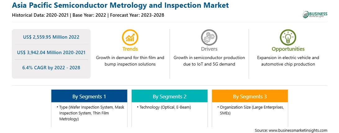
亚太地区半导体计量和检测市场根据类型、技术、组织规模和国家/地区进行细分。根据类型,亚太地区半导体计量和检测市场分为晶圆检测系统、掩模检测系统和薄膜计量。晶圆检测系统领域在 2022 年占据市场主导地位。根据技术,亚太地区半导体计量和检测市场分为光学和电子束。到 2022 年,光学领域将主导市场。根据组织规模,亚太地区半导体计量和检测市场分为大型企业和中小企业。大型企业细分市场将在 2022 年占据主导地位。根据国家/地区,亚太地区半导体计量和检测市场已细分为中国、印度、日本、韩国、台湾和亚太地区其他地区。 2022 年,中国将主导市场。
应用材料公司;阿斯麦控股公司;日立高新技术公司;日本电子有限公司; KLA 公司;激光技术公司;尼康计量公司;诺瓦有限公司;创新;和 Thermo Fisher Scientific Inc. 是亚太地区半导体计量和检测市场的领先公司之一。
Strategic insights for Asia Pacific Semiconductor Metrology and Inspection involve closely monitoring industry trends, consumer behaviours, and competitor actions to identify opportunities for growth. By leveraging data analytics, businesses can anticipate market shifts and make informed decisions that align with evolving customer needs. Understanding these dynamics helps companies adjust their strategies proactively, enhance customer engagement, and strengthen their competitive edge. Building strong relationships with stakeholders and staying agile in response to changes ensures long-term success in any market.
| Report Attribute | Details |
|---|---|
| Market size in 2022 | US$ 2,559.95 Million |
| Market Size by 2028 | US$ 3,942.04 Million |
| Global CAGR (2022 - 2028) | 6.4% |
| Historical Data | 2020-2021 |
| Forecast period | 2023-2028 |
| Segments Covered |
By 类型
|
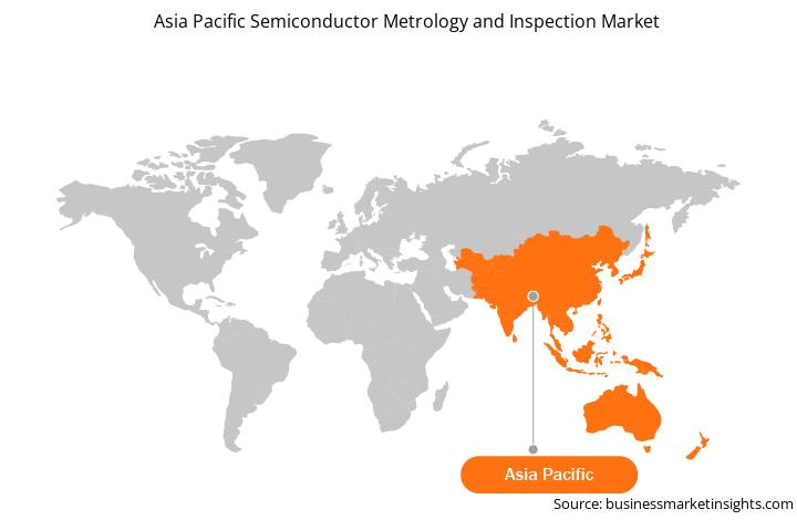
| Regions and Countries Covered | 亚太地区
|
| Market leaders and key company profiles |
The regional scope of Asia Pacific Semiconductor Metrology and Inspection refers to the geographical area in which a business operates and competes. Understanding regional nuances, such as local consumer preferences, economic conditions, and regulatory environments, is crucial for tailoring strategies to specific markets. Businesses can expand their reach by identifying underserved regions or adapting their offerings to meet regional demands. A clear regional focus allows for more effective resource allocation, targeted marketing, and better positioning against local competitors, ultimately driving growth in those specific areas.
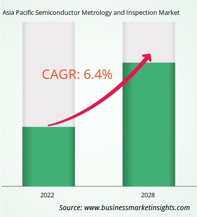
The Asia Pacific Semiconductor Metrology and Inspection Market is valued at US$ 2,559.95 Million in 2022, it is projected to reach US$ 3,942.04 Million by 2028.
As per our report Asia Pacific Semiconductor Metrology and Inspection Market, the market size is valued at US$ 2,559.95 Million in 2022, projecting it to reach US$ 3,942.04 Million by 2028. This translates to a CAGR of approximately 6.4% during the forecast period.
The Asia Pacific Semiconductor Metrology and Inspection Market report typically cover these key segments-
The historic period, base year, and forecast period can vary slightly depending on the specific market research report. However, for the Asia Pacific Semiconductor Metrology and Inspection Market report:
The Asia Pacific Semiconductor Metrology and Inspection Market is populated by several key players, each contributing to its growth and innovation. Some of the major players include:
The Asia Pacific Semiconductor Metrology and Inspection Market report is valuable for diverse stakeholders, including:
Essentially, anyone involved in or considering involvement in the Asia Pacific Semiconductor Metrology and Inspection Market value chain can benefit from the information contained in a comprehensive market report.
Office No. 1011, First floor, Farena Corporate Park, Magarpatta-Mundhwa road, Pune - 411028, Maharashtra, India
US:+16467917070
sales@businessmarketinsights.com


 Get Free Sample For Asia Pacific Semiconductor Metrology and Inspection Market
