1. Introduction
1.1 Business Market Insights Research Report Guidance
1.2 Market Segmentation
2. Executive Summary
2.1 Key Market Insights
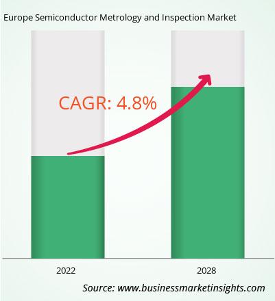
2.2 Market Attractiveness
3. Research Methodology
3.1 Secondary Research
3.2 Primary Research
- 3.2.1 Hypothesis formulation:
- 3.2.2 Macro-economic factor analysis:
- 3.2.3 Developing base number:
- 3.2.4 Data Triangulation:
- 3.2.5 Country level data:
4. Europe Semiconductor Metrology and Inspection Market Landscape
4.1 Market Overview
4.2 Porter's Five Forces Analysis
- 4.2.1 Bargaining Power of Suppliers
- 4.2.2 Bargaining Power of Buyers
- 4.2.3 Threat of New Entrants
- 4.2.4 Competitive Rivalry
- 4.2.5 Threat of Substitutes
4.3 Ecosystem Analysis
- 4.3.1 Raw Material Suppliers
- 4.3.2 Manufacturers
- 4.3.3 Distributors/Suppliers
- 4.3.4 End Users
5. Europe Semiconductor Metrology and Inspection Market – Key Market Dynamics
5.1 Growth Drivers
- 5.1.1 Growth in semiconductor production due to IoT and 5G demand
- 5.1.2 Need for precision and defect detection in advanced chips
5.2 Market Opportunities
- 5.2.1 Expansion in electric vehicle and automotive chip production
- 5.2.2 Adoption of automated inspection solutions for enhanced productivity
5.3 Future Trends
- 5.3.1 Growth in demand for thin film and bump inspection solutions
- 5.3.2 Shift toward integrated metrology systems for real-time feedback
5.4 Impact of Drivers and Restraints
6. Europe Semiconductor Metrology and Inspection Market Regional Analysis
6.1 Europe Semiconductor Metrology and Inspection Market Overview
6.2 Europe Semiconductor Metrology and Inspection Market Revenue 2020-2028 (US$ Million)
6.3 Europe Semiconductor Metrology and Inspection Market Forecast Analysis
7. Europe Semiconductor Metrology and Inspection Market Analysis – by Type
7.1 Wafer Inspection System
- 7.1.1 Overview
- 7.1.2 Wafer Inspection System: Europe Semiconductor Metrology and Inspection Market – Revenue and Forecast to 2031 (US$ Million)
7.2 Mask Inspection System
- 7.2.1 Overview
- 7.2.2 Mask Inspection System: Europe Semiconductor Metrology and Inspection Market – Revenue and Forecast to 2031 (US$ Million)
7.3 Thin Film Metrology
- 7.3.1 Overview
- 7.3.2 Thin Film Metrology: Europe Semiconductor Metrology and Inspection Market – Revenue and Forecast to 2031 (US$ Million)
8. Europe Semiconductor Metrology and Inspection Market Analysis – by Technology
8.1 Optical
- 8.1.1 Overview
- 8.1.2 Optical: Europe Semiconductor Metrology and Inspection Market – Revenue and Forecast to 2028 (US$ Million)
8.2 E-Beam
- 8.2.1 Overview
- 8.2.2 E-Beam: Europe Semiconductor Metrology and Inspection Market – Revenue and Forecast to 2028 (US$ Million)
9. Europe Semiconductor Metrology and Inspection Market Analysis – by Organization Size
9.1 Large Enterprises
- 9.1.1 Overview
- 9.1.2 E-Beam: Europe Semiconductor Metrology and Inspection Market – Revenue and Forecast to 2028 (US$ Million)
9.2 SMEs
- 9.2.1 Overview
- 9.2.2 E-Beam: Europe Semiconductor Metrology and Inspection Market – Revenue and Forecast to 2028 (US$ Million)
10. Europe Semiconductor Metrology and Inspection Market – Europe Analysis
10.1 Europe
- 10.1.1 Europe Semiconductor Metrology and Inspection Market Breakdown, by Key
Country, 2023 and 2028 (%)
- 10.1.1.1 Europe Semiconductor Metrology and Inspection Market – Revenue and
Forecast Analysis – by Country
- 10.1.1.1 UK:
Europe Semiconductor Metrology and Inspection Market – Revenue and Forecast to 2028 (US$ Million)
- 10.1.1.1.1 UK: Europe Semiconductor Metrology and Inspection Market Breakdown, by Type
- 10.1.1.1.2 UK: Europe Semiconductor Metrology and Inspection Market Breakdown, by Technology
- 10.1.1.1.3 UK: Europe Semiconductor Metrology and Inspection Market Breakdown, by Organization Size
- 10.1.1.2 Germany:
Europe Semiconductor Metrology and Inspection Market – Revenue and Forecast to 2028 (US$ Million)
- 10.1.1.2.1 Germany: Europe Semiconductor Metrology and Inspection Market Breakdown, by Type
- 10.1.1.2.2 Germany: Europe Semiconductor Metrology and Inspection Market Breakdown, by Technology
- 10.1.1.2.3 Germany: Europe Semiconductor Metrology and Inspection Market Breakdown, by Organization Size
- 10.1.1.3 France:
Europe Semiconductor Metrology and Inspection Market – Revenue and Forecast to 2028 (US$ Million)
- 10.1.1.3.1 France: Europe Semiconductor Metrology and Inspection Market Breakdown, by Type
- 10.1.1.3.2 France: Europe Semiconductor Metrology and Inspection Market Breakdown, by Technology
- 10.1.1.3.3 France: Europe Semiconductor Metrology and Inspection Market Breakdown, by Organization Size
- 10.1.1.4 Russia:
Europe Semiconductor Metrology and Inspection Market – Revenue and Forecast to 2028 (US$ Million)
- 10.1.1.4.1 Russia: Europe Semiconductor Metrology and Inspection Market Breakdown, by Type
- 10.1.1.4.2 Russia: Europe Semiconductor Metrology and Inspection Market Breakdown, by Technology
- 10.1.1.4.3 Russia: Europe Semiconductor Metrology and Inspection Market Breakdown, by Organization Size
- 10.1.1.5 Italy:
Europe Semiconductor Metrology and Inspection Market – Revenue and Forecast to 2028 (US$ Million)
- 10.1.1.5.1 Italy: Europe Semiconductor Metrology and Inspection Market Breakdown, by Type
- 10.1.1.5.2 Italy: Europe Semiconductor Metrology and Inspection Market Breakdown, by Technology
- 10.1.1.5.3 Italy: Europe Semiconductor Metrology and Inspection Market Breakdown, by Organization Size
- 10.1.1.6 Rest of Europe:
Europe Semiconductor Metrology and Inspection Market – Revenue and Forecast to 2028 (US$ Million)
- 10.1.1.6.1 Rest of Europe: Europe Semiconductor Metrology and Inspection Market Breakdown, by Type
- 10.1.1.6.2 Rest of Europe: Europe Semiconductor Metrology and Inspection Market Breakdown, by Technology
- 10.1.1.6.3 Rest of Europe: Europe Semiconductor Metrology and Inspection Market Breakdown, by Organization Size
11. Competitive Landscape
11.1 Heat Map Analysis
11.2 Company Positioning and Concentration
12. Europe Semiconductor Metrology and Inspection Market Industry Landscape
12.1 Overview
12.2 Mergers and Acquisitions
12.3 Agreements, Collaborations, and Joint Ventures
12.4 New Product Launches
12.5 Expansions and Other Strategic Developments
13. Company Profiles
13.1 Applied Materials, Inc.
- 13.1.1 Key Facts
- 13.1.2 Business Description
- 13.1.3 Products and Services
- 13.1.4 Financial Overview
- 13.1.5 SWOT Analysis
- 13.1.6 Key Developments
13.2 ASML Holding N.V.
- 13.2.1 Key Facts
- 13.2.2 Business Description
- 13.2.3 Products and Services
- 13.2.4 Financial Overview
- 13.2.5 SWOT Analysis
- 13.2.6 Key Developments
13.3 Hitachi High-Tech Corporation
- 13.3.1 Key Facts
- 13.3.2 Business Description
- 13.3.3 Products and Services
- 13.3.4 Financial Overview
- 13.3.5 SWOT Analysis
- 13.3.6 Key Developments
13.4 JEOL Ltd
- 13.4.1 Key Facts
- 13.4.2 Business Description
- 13.4.3 Products and Services
- 13.4.4 Financial Overview
- 13.4.5 SWOT Analysis
- 13.4.6 Key Developments
13.5 KLA Corporation
- 13.5.1 Key Facts
- 13.5.2 Business Description
- 13.5.3 Products and Services
- 13.5.4 Financial Overview
- 13.5.5 SWOT Analysis
- 13.5.6 Key Developments
13.6 Lasertec Corporation
- 13.6.1 Key Facts
- 13.6.2 Business Description
- 13.6.3 Products and Services
- 13.6.4 Financial Overview
- 13.6.5 SWOT Analysis
- 13.6.6 Key Developments
13.7 Nikon Metrology NV
- 13.7.1 Key Facts
- 13.7.2 Business Description
- 13.7.3 Products and Services
- 13.7.4 Financial Overview
- 13.7.5 SWOT Analysis
- 13.7.6 Key Developments
13.8 Nova Ltd.
- 13.8.1 Key Facts
- 13.8.2 Business Description
- 13.8.3 Products and Services
- 13.8.4 Financial Overview
- 13.8.5 SWOT Analysis
- 13.8.6 Key Developments
13.9 Onto Innovation
- 13.9.1 Key Facts
- 13.9.2 Business Description
- 13.9.3 Products and Services
- 13.9.4 Financial Overview
- 13.9.5 SWOT Analysis
- 13.9.6 Key Developments
13.10 Thermo Fisher Scientific Inc.
- 13.10.1 Key Facts
- 13.10.2 Business Description
- 13.10.3 Products and Services
- 13.10.4 Financial Overview
- 13.10.5 SWOT Analysis
- 13.10.6 Key Developments
14. Appendix
14.1 About Business Market Insights


 Get Free Sample For Europe Semiconductor Metrology and Inspection Market

