Europe Semiconductor Metrology and Inspection Market
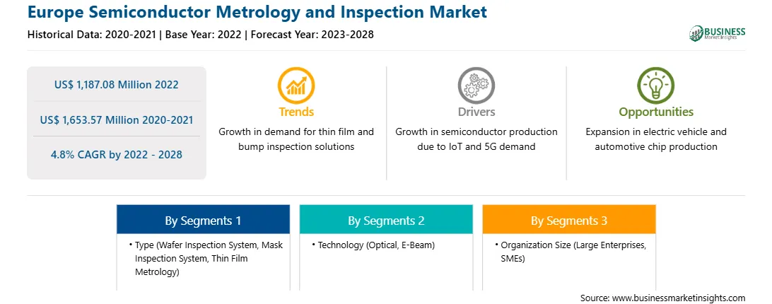
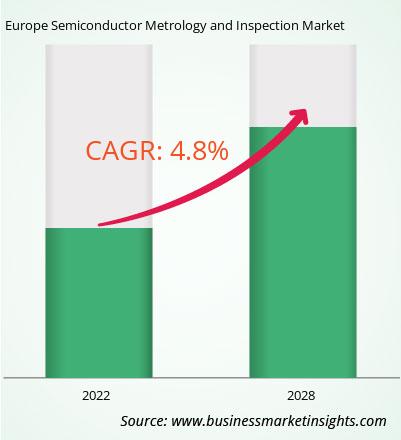
The Europe semiconductor metrology and inspection market is expected to grow from US$ 1,187.08 million in 2022 to US$ 1,653.57 million by 2028; it is estimated to grow at a CAGR of 4.8% from 2022 to 2028.
Wafer fabrication, manufacturing, and other procedures use advanced packaging (AP) technology. Controlling these operations in the back end necessitates inspection and measurement methods. Shrinking feature sizes are driving the demand for high accuracy, precision, sensitivity, and throughput. On the other hand, AP procedures face measurement and inspection issues, such as bump metrology and nonvisual flaws, that are unique to back-end applications. Special requirements, combined with the increased diversity and rapid evolution of AP processes, propel the demand for flexible measurement and inspection systems that can control a wide range of parameters, including two-dimensional (2D) and three-dimensional (3D) geometries, and can be adapted to new requirements as they arise. Combining various competencies into a single platform is the most economical and effective use of capital. Keeping up with the industry's roadmap necessitates novel solutions from equipment providers focusing on the unique requirements of AP operations. For example, KLA Corporation offers Kronos 1190 patterned wafer inspection system with high-resolution optics in advanced wafer-level packaging (AWLP) applications such as 3D IC and high-density fan-out. The system gives sensitivity to important flaws for process development and production monitoring. Manufacturers are under pressure to improve quality and dependability. This is especially true in industries such as automotive, where consumer safety is a major concern. Thousands of semiconductor components exist in autos. In addition, the number of components might increase by orders of magnitude in completely driverless vehicles. For a car with 10,000 components, a component failure rate of one in a million amounts to a vehicle failure rate of one in 100, which is unacceptable. To meet this challenge in current and next-generation packages, defect sensitivity down to the micrometer level and the ability to discern lethal faults swiftly and consistently amid massive raw data streams are required. Gauge repeatability and reproducibility (R&R) investigations are becoming relevant. Engineers need technologies to turn raw data into useful process knowledge. E-beam technology is also being adopted in advanced packaging. Electrons are created within the tool in an e-beam inspection system and then hit the surface of a die. The electrons scatter and bounce back to a detector, allowing it to detect chips with faults.
With the new features and technologies, vendors can attract new customers and expand their footprints in emerging markets. This factor is likely to drive the Europe semiconductor metrology and inspection market. The Europe semiconductor metrology and inspection market is expected to grow at a good CAGR during the forecast period.
Europe Semiconductor Metrology and Inspection Market Revenue and Forecast to 2028 (US$ Million)
Strategic insights for the Europe Semiconductor Metrology and Inspection provides data-driven analysis of the industry landscape, including current trends, key players, and regional nuances. These insights offer actionable recommendations, enabling readers to differentiate themselves from competitors by identifying untapped segments or developing unique value propositions. Leveraging data analytics, these insights help industry players anticipate the market shifts, whether investors, manufacturers, or other stakeholders. A future-oriented perspective is essential, helping stakeholders anticipate market shifts and position themselves for long-term success in this dynamic region. Ultimately, effective strategic insights empower readers to make informed decisions that drive profitability and achieve their business objectives within the market. The geographic scope of the Europe Semiconductor Metrology and Inspection refers to the specific areas in which a business operates and competes. Understanding local distinctions, such as diverse consumer preferences (e.g., demand for specific plug types or battery backup durations), varying economic conditions, and regulatory environments, is crucial for tailoring strategies to specific markets. Businesses can expand their reach by identifying underserved areas or adapting their offerings to meet local demands. A clear market focus allows for more effective resource allocation, targeted marketing campaigns, and better positioning against local competitors, ultimately driving growth in those targeted areas. Get more information on this report
 Europe Semiconductor Metrology and Inspection Strategic Insights
 Get more information on this report
 Europe Semiconductor Metrology and Inspection Report Scope
Report Attribute
Details
Market size in 2022
US$ 1,187.08 Million
Market Size by 2028
US$ 1,653.57 Million
Global CAGR (2022 - 2028)
4.8%
Historical Data
2020-2021
Forecast period
2023-2028
Segments Covered
By Type
By Technology
By Organization Size
Regions and Countries Covered
Europe
Market leaders and key company profiles
Get more information on this report Europe Semiconductor Metrology and Inspection Regional Insights
 Get more information on this report
Europe Semiconductor Metrology and Inspection Market Segmentation
The Europe semiconductor metrology and inspection market is segmented based on type, technology, organization size, and country. Based on type, the Europe semiconductor metrology and inspection market is segmented into wafer inspection system, mask inspection system, and thin film metrology. The wafer inspection system segment dominated the market in 2022. Based on technology, the Europe semiconductor metrology and inspection market is bifurcated into optical and e-beam. The optical segment dominated the market in 2022. Based on organization size, the Europe semiconductor metrology and inspection market is bifurcated into large enterprises and SMEs. The large enterprises segment dominated the market in 2022. Based on country, the Europe semiconductor metrology and inspection market has been segmented into the UK, Germany, France, Italy, Russia, and the Rest of Europe. Germany dominated the market in 2022.
Applied Materials, Inc.; ASML Holding N.V.; Hitachi High-Tech Corporation; JEOL Ltd; KLA Corporation; Lasertec Corporation; Nikon Metrology NV; Nova Ltd.; Onto Innovation; and Thermo Fisher Scientific Inc. are among the leading companies in the Europe semiconductor metrology and inspection market.
The Europe Semiconductor Metrology and Inspection Market is valued at US$ 1,187.08 Million in 2022, it is projected to reach US$ 1,653.57 Million by 2028.
As per our report Europe Semiconductor Metrology and Inspection Market, the market size is valued at US$ 1,187.08 Million in 2022, projecting it to reach US$ 1,653.57 Million by 2028. This translates to a CAGR of approximately 4.8% during the forecast period.
The Europe Semiconductor Metrology and Inspection Market report typically cover these key segments-
The historic period, base year, and forecast period can vary slightly depending on the specific market research report. However, for the Europe Semiconductor Metrology and Inspection Market report:
The Europe Semiconductor Metrology and Inspection Market is populated by several key players, each contributing to its growth and innovation. Some of the major players include:
The Europe Semiconductor Metrology and Inspection Market report is valuable for diverse stakeholders, including:
Essentially, anyone involved in or considering involvement in the Europe Semiconductor Metrology and Inspection Market value chain can benefit from the information contained in a comprehensive market report.
Office No. 1011, First floor, Farena Corporate Park, Magarpatta-Mundhwa road, Pune - 411028, Maharashtra, India
US:+16467917070
sales@businessmarketinsights.com


 Get Free Sample For Europe Semiconductor Metrology and Inspection Market
