Asia Pacific Silicon EPI Wafer Market
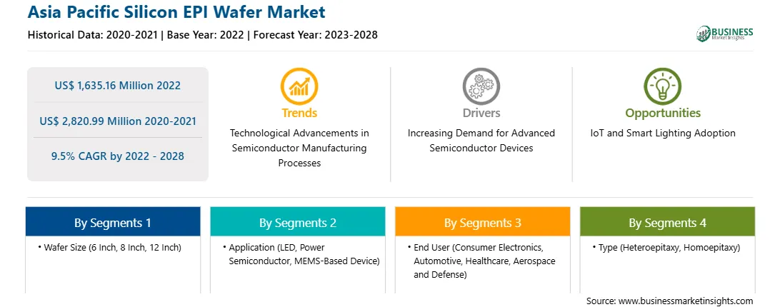
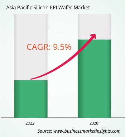
The Asia Pacific silicon EPI wafer market is expected to grow from US$ 1,635.16 million in 2022 to US$ 2,820.99 million by 2028; it is estimated to grow at a CAGR of 9.5% from 2022 to 2028.
Gallium nitride (GaN), a wide bandgap semiconductor, supports the functioning of devices at higher temperatures and voltages than silicon-based devices. The greater dielectric breakdown of GaN also makes it possible to build smaller devices with lower resistance. Lower resistance leads to smaller devices with less capacitance (on). Epitaxial GaN wafers, characterized by high efficiency and high-power output, are a base material used in power and radio frequency (RF) devices. They are used in defense radars, electric car power converters, 5G base stations, and quick chargers for IT devices. For instance, IVWorks, South Korea, makes GaN epitaxial wafers a crucial component of DC power devices and 5G communication devices by using deep learning-based artificial intelligence (AI) epitaxy technology, further attracting a US$ 6.7 million Series B investment. Due to their high electron mobility, current density, and breakdown voltage, GaN can be used to create high-efficiency, high-output power devices that operate at a high frequency. It is smaller, quicker, and more efficient than Si, SiC, and GaAs materials, and produces more power than these materials. GaN epitaxial growth is necessary on a heterogeneous substrate since GaN has not yet been adequately developed in free-standing wafer technology, unlike Si, SiC, and GaAs (Si or SiC). Although Si can affordably handle wafers with enormous diameters, a technique to manage stress and defect density is required because of the huge lattice mismatch and thermal expansion coefficient difference from GaN. Continuous advancements in AI-based GaN wafers are providing lucrative opportunities for the future growth of the silicon EPI wafer market.
Vendors in the Asia-Pacific silicon EPI wafer market can attract new customers and expand their footprints in emerging markets by providing innovative products. This is likely to drive market at a notable CAGR during the forecast period.
Strategic insights for the Asia Pacific Silicon EPI Wafer provides data-driven analysis of the industry landscape, including current trends, key players, and regional nuances. These insights offer actionable recommendations, enabling readers to differentiate themselves from competitors by identifying untapped segments or developing unique value propositions. Leveraging data analytics, these insights help industry players anticipate the market shifts, whether investors, manufacturers, or other stakeholders. A future-oriented perspective is essential, helping stakeholders anticipate market shifts and position themselves for long-term success in this dynamic region. Ultimately, effective strategic insights empower readers to make informed decisions that drive profitability and achieve their business objectives within the market. The geographic scope of the Asia Pacific Silicon EPI Wafer refers to the specific areas in which a business operates and competes. Understanding local distinctions, such as diverse consumer preferences (e.g., demand for specific plug types or battery backup durations), varying economic conditions, and regulatory environments, is crucial for tailoring strategies to specific markets. Businesses can expand their reach by identifying underserved areas or adapting their offerings to meet local demands. A clear market focus allows for more effective resource allocation, targeted marketing campaigns, and better positioning against local competitors, ultimately driving growth in those targeted areas. Get more information on this report
 Asia Pacific Silicon EPI Wafer Strategic Insights
 Get more information on this report
 Asia Pacific Silicon EPI Wafer Report Scope
Report Attribute
Details
Market size in 2022
US$ 1,635.16 Million
Market Size by 2028
US$ 2,820.99 Million
Global CAGR (2022 - 2028)
9.5%
Historical Data
2020-2021
Forecast period
2023-2028
Segments Covered
By Wafer Size
By Application
By End User
By Type
Regions and Countries Covered
Asia-Pacific
Market leaders and key company profiles
Get more information on this report Asia Pacific Silicon EPI Wafer Regional Insights
 Get more information on this report
Asia-Pacific Silicon EPI Wafer Market Segmentation
The Asia-Pacific silicon EPI wafer market is segmented on the basis of wafer size, application, end user, type, and country. Based on wafer size, the market is segmented into 6 inch, 8 inch, 12 inch, and others. Based on application, the market is divided into led, power semiconductor, and MEMS-based devices. By end user, the Asia-Pacific silicon EPI wafer market is segmented into consumer electronics, automotive, healthcare, aerospace and defense, and others. Based on type, the market is bifurcated into heteroepitaxy and homoepitaxy. Based on country, the Asia Pacific silicon EPI wafer market is segmented into Taiwan, China, India, Japan, South Korea, and Rest of Asia Pacific.
Asia Pacific Silicon EPI Wafer Market — Companies Mentioned
Applied Materials, Inc.; II-VI Incorporated; Shin-Etsu Chemical Co., Ltd.; SUMCO CORPORATION; Siltronic AG; NICHIA CORPORATION; GlobalWafers Japan Co., Ltd.; EpiGaN nv (Soitec Belgium N.V.) and SK Siltron Co., Ltd. are among the major companies operating in the Asia-Pacific silicon EPI wafer market.
The Asia Pacific Silicon EPI Wafer Market is valued at US$ 1,635.16 Million in 2022, it is projected to reach US$ 2,820.99 Million by 2028.
As per our report Asia Pacific Silicon EPI Wafer Market, the market size is valued at US$ 1,635.16 Million in 2022, projecting it to reach US$ 2,820.99 Million by 2028. This translates to a CAGR of approximately 9.5% during the forecast period.
The Asia Pacific Silicon EPI Wafer Market report typically cover these key segments-
The historic period, base year, and forecast period can vary slightly depending on the specific market research report. However, for the Asia Pacific Silicon EPI Wafer Market report:
The Asia Pacific Silicon EPI Wafer Market is populated by several key players, each contributing to its growth and innovation. Some of the major players include:
The Asia Pacific Silicon EPI Wafer Market report is valuable for diverse stakeholders, including:
Essentially, anyone involved in or considering involvement in the Asia Pacific Silicon EPI Wafer Market value chain can benefit from the information contained in a comprehensive market report.
Office No. 1011, First floor, Farena Corporate Park, Magarpatta-Mundhwa road, Pune - 411028, Maharashtra, India
US:+16467917070
sales@businessmarketinsights.com


 Get Free Sample For Asia Pacific Silicon EPI Wafer Market
