2028년까지 유럽 반도체 본딩 시장 전망 - 코로나19 영향 및 유형(다이 본더, 웨이퍼 본더, 플립 칩 본더) 및 애플리케이션(RF 장치, MEMS 및 센서, LED, CMOS 이미지 센서 및 3D NAND)별 지역 분석
No. of Pages: 123 | Report Code: BMIRE00027611 | Category: Electronics and Semiconductor
No. of Pages: 123 | Report Code: BMIRE00027611 | Category: Electronics and Semiconductor
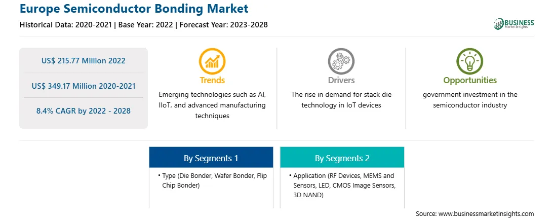
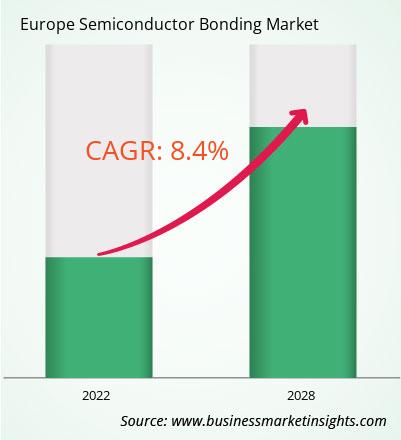
유럽의 반도체 본딩 시장은 2022년 2억 1,577만 달러에서 2028년 3억 4,917만 달러로 성장할 것으로 예상됩니다. 2022년부터 2028년까지 연평균 성장률(CAGR) 8.4%로 성장할 것으로 예상됩니다. .
소형 인쇄 회로 기판(PCB)의 향상된 기능과 성능에 대한 OEM의 요구가 증가함에 따라 IoT 및 모바일 장치와 같은 다양한 전자 애플리케이션에서 스택 다이 기술의 채택이 증가했습니다. 스택형 다이는 하나의 칩을 다른 칩 위에 배치하거나 칩 대신 스페이서를 배치한 후 다른 칩을 배치하는 것을 의미합니다. 여러 행의 와이어 본딩 루프 세트가 배열되어 있으며 각 세트는 서로 다른 다이 또는 스페이서에 연결됩니다. 따라서 적층된 다이 이후 남은 공간은 작은 다이 배치 영역에 많은 기능을 맞추는 데 사용됩니다. 따라서 스택 다이 기술을 사용하여 회로를 배치하면 귀중한 PCB 공간을 보존하는 데 도움이 됩니다. PCB 조립 및 제조 회사가 극도로 견고하고 견고한 플렉스 회로를 경험한 제한된 작업 공간으로 인해 IoT 장치에서 스택 다이 기술에 대한 수요가 증가하고 있습니다. 또한 적층형 다이를 사용하면 반도체 설계 프로세스가 크게 향상됩니다. Stacked Die 기술은 소형 최종 디자인을 제작하는 데 사용됩니다. 적층 다이 기술을 발전시키는 주요 요인 중 하나는 휴대용 전자 장치입니다. 또한 실시간 추적 IoT 장치도 거대할 수 없습니다. 설계 노력을 줄이고 최초 성공 가능성을 높이면 출시 기간이 단축됩니다. 따라서 IoT 장치에서 적층 다이 기술의 채택이 증가함에 따라 시장에서 반도체 본딩 솔루션에 대한 수요가 높아지고 있습니다. 또한, 반도체 부문의 OEM은 연결성을 넘어 IoT의 이점을 활용하고 있습니다. 센서, RFID 태그, 스마트 비콘, 스마트 미터, 유통 제어 시스템은 빌딩 및 홈 자동화, 연결된 물류, 스마트 제조, 스마트 소매, 스마트 모빌리티, 스마트 교통 등 다양한 애플리케이션에서 점점 더 많이 사용되고 있는 IoT 장치 및 기술입니다. . 사물 인터넷(IoT) 장치에서는 반도체 본딩 기술을 활용하여 여러 개의 적층된 다이를 기판에 콤팩트하게 부착하는데, 이는 유럽 반도체 본딩 시장의 성장으로 이어질 것입니다.
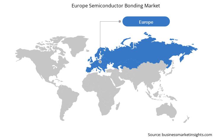
독일, 프랑스, 이탈리아, 러시아, 영국 및 기타 유럽 국가가 주요 기여자입니다. 유럽 반도체 본딩 시장 진출 스택형 다이(Stacked Die)는 하나의 반도체 패키지에 두 개 이상의 다이(Die)를 쌓아서 접합하는 조립 기술이다. 동일한 배치 영역 주위에 다양한 기능을 갖는 기판에 사용됩니다. 다이 파일링으로 인해 전기 장치의 성능이 향상됩니다. 따라서 적층 다이의 활용은 시장 성장을 가속화하는 주요 동인 중 하나입니다. EV 그룹, HUTEM은 유럽 반도체 본딩 시장에서 활동하는 저명한 회사 중 일부입니다. 이들 회사는 주로 MEMS 센서, CMOS 이미지 센서, RF 장치 시장에 주력하고 있습니다. 예를 들어, 2022년 3월 독일 소재 제약회사인 Merck KGaA는 중국 장자강에 새로운 반도체 시설을 건설하기 위해 총 8,200만 달러를 투자한다고 발표했습니다. 웨이퍼 본딩의 성장은 군용 및 보안용 야간 투시경 시스템, 건물 건설 개선을 위한 이미징 시스템, 자동차 보행자 보호 시스템용 열 카메라, 여러 상업용 프로세스 모니터링 시스템을 비롯한 다양한 열 이미징 애플리케이션에 대한 수요 증가로 인해 가속화되었습니다. 그리고 산업 응용. MEMS 제조업체에는 수요를 충족하는 데 필요한 단위 비용 절감을 달성하기 위해 높은 처리량과 수율로 마이크로볼로미터를 생산할 수 있는 고급 공정 장비와 전문 지식이 필요합니다. EV Group(EVG)의 완전 자동화된 GEMINI 웨이퍼 본더를 사용하면 마이크로볼로미터를 비용 효율적으로 생산할 수 있습니다. 마찬가지로 2020년 10월 오스트리아에서 EVG는 3D 반도체 패키징을 위해 2μm 미만의 배치 정확도를 갖춘 D2W(다이-웨이퍼) 하이브리드 및 융합 결합을 위한 완전한 프로세스 흐름을 확립했습니다.
유럽 반도체 본딩 시장 수익 및 2028년 예측(미화 백만 달러)
유럽 반도체 본딩 시장 세분화
유럽 반도체 본딩 시장은 유형, 애플리케이션 및 국가로 분류됩니다.
ASMPT; DIAS Automation (HK) Ltd.; EV그룹; 휴템; 쿨리케 & 소파 인더스트리즈(Soffa Industries, Inc.); 팔로마 테크놀로지스; 파나소닉 주식회사; 도레이 산업(주); 웨스트본드, Inc.; Yamaha Motor Corporation은 유럽 지역의 반도체 본딩 시장에서 활동하는 선두 기업입니다.
Strategic insights for Europe Semiconductor Bonding involve closely monitoring industry trends, consumer behaviours, and competitor actions to identify opportunities for growth. By leveraging data analytics, businesses can anticipate market shifts and make informed decisions that align with evolving customer needs. Understanding these dynamics helps companies adjust their strategies proactively, enhance customer engagement, and strengthen their competitive edge. Building strong relationships with stakeholders and staying agile in response to changes ensures long-term success in any market.
| Report Attribute | Details |
|---|---|
| Market size in 2022 | US$ 215.77 Million |
| Market Size by 2028 | US$ 349.17 Million |
| Global CAGR (2022 - 2028) | 8.4% |
| Historical Data | 2020-2021 |
| Forecast period | 2023-2028 |
| Segments Covered |
By 종류
|
| Regions and Countries Covered | 유럽
|
| Market leaders and key company profiles |
The regional scope of Europe Semiconductor Bonding refers to the geographical area in which a business operates and competes. Understanding regional nuances, such as local consumer preferences, economic conditions, and regulatory environments, is crucial for tailoring strategies to specific markets. Businesses can expand their reach by identifying underserved regions or adapting their offerings to meet regional demands. A clear regional focus allows for more effective resource allocation, targeted marketing, and better positioning against local competitors, ultimately driving growth in those specific areas.
The Europe Semiconductor Bonding Market is valued at US$ 215.77 Million in 2022, it is projected to reach US$ 349.17 Million by 2028.
As per our report Europe Semiconductor Bonding Market, the market size is valued at US$ 215.77 Million in 2022, projecting it to reach US$ 349.17 Million by 2028. This translates to a CAGR of approximately 8.4% during the forecast period.
The Europe Semiconductor Bonding Market report typically cover these key segments-
The historic period, base year, and forecast period can vary slightly depending on the specific market research report. However, for the Europe Semiconductor Bonding Market report:
The Europe Semiconductor Bonding Market is populated by several key players, each contributing to its growth and innovation. Some of the major players include:
The Europe Semiconductor Bonding Market report is valuable for diverse stakeholders, including:
Essentially, anyone involved in or considering involvement in the Europe Semiconductor Bonding Market value chain can benefit from the information contained in a comprehensive market report.
Office No. 1011, First floor, Farena Corporate Park, Magarpatta-Mundhwa road, Pune - 411028, Maharashtra, India
US:+16467917070
sales@businessmarketinsights.com


 Get Free Sample For Europe Semiconductor Bonding Market
