2028년까지 아시아 태평양 반도체 계측 및 검사 시장 예측 – 유형(웨이퍼 검사 시스템, 마스크 검사 시스템 및 박막 계측), 기술(광학 및 전자빔)별 코로나19 영향 및 지역 분석 조직 규모(대기업 및 중소기업)
No. of Pages: 126 | Report Code: BMIRE00027255 | Category: Electronics and Semiconductor
No. of Pages: 126 | Report Code: BMIRE00027255 | Category: Electronics and Semiconductor
APAC는 반도체 산업 측면에서 가장 중요한 지역 중 하나입니다. 제조 및 활용. SIA(반도체산업협회)에 따르면 APAC는 가장 큰 지역 반도체 시장이며, 중국은 단일 국가 최대 시장입니다. 반도체 계측/검사장비 산업에서는 많은 기업들이 제휴 및 파트너십을 맺고 있습니다. 예를 들어, 중국 칩 제조 도구 제조업체인 Shenzhen JT Automation Equipment는 2021년 7월 Huawei의 HiSilicon Technologies Company와 법적 구속력이 있는 5년 계약을 체결했습니다. 두 회사 모두 반도체 패키징 도구 개발 관계를 발전시키고 해당 부문을 자체화하기를 원합니다. -충분하고 규제됩니다. 따라서 이번 파트너십을 통해 패키징 기술에 반도체 사용이 증가할 것입니다. APAC의 많은 시장 참가자들이 시장에 혁신적인 제품을 출시하고 있습니다. 예를 들어 Hitachi High-Tech Corporation은 2020년 11월에 SEM*1 CR7300 고속 결함 검사를 출시했습니다. CR7300은 반도체 장치 제조 생산성 향상에 도움이 되는 새로운 검토 SEM 유형입니다. 이는 최고의 고해상도 사진 획득을 가능하게 하는 전자 광학을 기반으로 합니다. 동시에 새로운 이미징 및 스테이지 기술을 사용하면 기존 방법에 비해 절반의 시간으로 고속 이미지를 획득할 수 있어 전체 검사 시간이 상당히 단축됩니다. 위에서 언급한 기술 혁신은 예측 기간 동안 APAC의 반도체 계측 및 검사 시장 참여자에게 기회를 창출할 것으로 예상됩니다.
새로운 기능과 기술을 통해 공급업체는 다음을 수행할 수 있습니다. 새로운 고객을 유치하고 신흥 시장에서 입지를 확장하세요. 이 요인은 APAC 반도체 계측 및 검사 시장을 주도할 가능성이 높습니다. APAC 반도체 계측 및 검사 시장은 예측 기간 동안 양호한 CAGR로 성장할 것으로 예상됩니다.
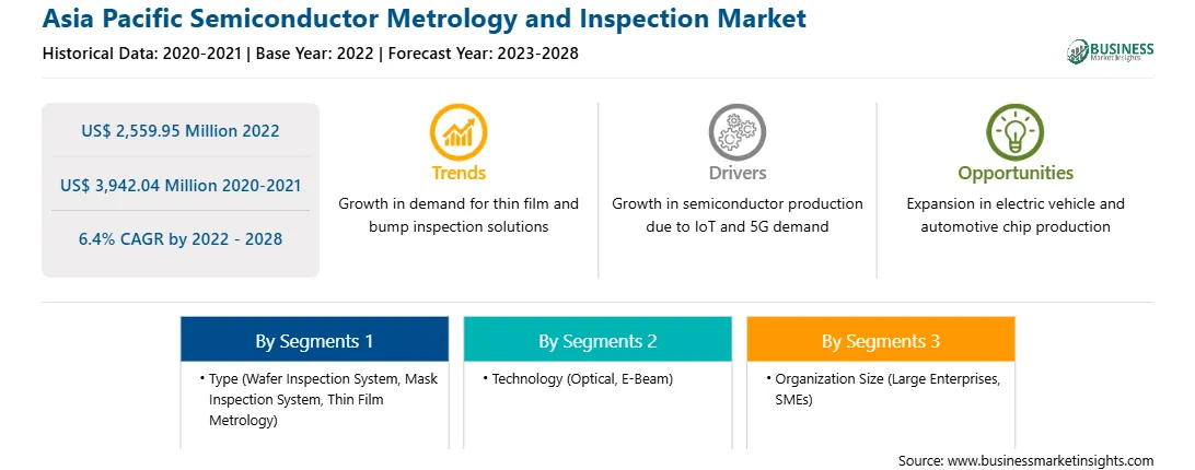
APAC 반도체 계측 및 검사 시장은 유형, 기술, 조직 규모 및 국가를 기준으로 분류됩니다. 유형에 따라 APAC 반도체 계측 및 검사 시장은 웨이퍼 검사 시스템, 마스크 검사 시스템 및 박막 계측으로 분류됩니다. 2022년에는 웨이퍼 검사 시스템 부문이 시장을 지배했습니다. 기술을 기반으로 APAC 반도체 계측 및 검사 시장은 광학 및 전자빔으로 구분됩니다. 2022년에는 광학 부문이 시장을 지배했습니다. 조직 규모에 따라 APAC 반도체 계측 및 검사 시장은 대기업과 중소기업으로 구분됩니다. 2022년에는 대기업 부문이 시장을 장악했습니다. 국가별로 APAC 반도체 계측 및 검사 시장은 중국, 인도, 일본, 한국, 대만 및 나머지 APAC 지역으로 분류되었습니다. 2022년에는 중국이 시장을 장악했습니다.
Applied Materials, Inc.; ASML 홀딩 NV; 히타치하이테크주식회사; JEOL Ltd; KLA 공사; 레이저텍 주식회사; 니콘 메트롤로지 NV; 노바 주식회사; 혁신에; 및 Thermo Fisher Scientific Inc.는 APAC 반도체 계측 및 검사 시장의 선두 기업 중 하나입니다.
Strategic insights for Asia Pacific Semiconductor Metrology and Inspection involve closely monitoring industry trends, consumer behaviours, and competitor actions to identify opportunities for growth. By leveraging data analytics, businesses can anticipate market shifts and make informed decisions that align with evolving customer needs. Understanding these dynamics helps companies adjust their strategies proactively, enhance customer engagement, and strengthen their competitive edge. Building strong relationships with stakeholders and staying agile in response to changes ensures long-term success in any market.
| Report Attribute | Details |
|---|---|
| Market size in 2022 | US$ 2,559.95 Million |
| Market Size by 2028 | US$ 3,942.04 Million |
| Global CAGR (2022 - 2028) | 6.4% |
| Historical Data | 2020-2021 |
| Forecast period | 2023-2028 |
| Segments Covered |
By 유형
|
| Regions and Countries Covered | 아시아 태평양
|
| Market leaders and key company profiles |
The regional scope of Asia Pacific Semiconductor Metrology and Inspection refers to the geographical area in which a business operates and competes. Understanding regional nuances, such as local consumer preferences, economic conditions, and regulatory environments, is crucial for tailoring strategies to specific markets. Businesses can expand their reach by identifying underserved regions or adapting their offerings to meet regional demands. A clear regional focus allows for more effective resource allocation, targeted marketing, and better positioning against local competitors, ultimately driving growth in those specific areas.
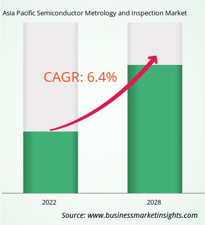
The Asia Pacific Semiconductor Metrology and Inspection Market is valued at US$ 2,559.95 Million in 2022, it is projected to reach US$ 3,942.04 Million by 2028.
As per our report Asia Pacific Semiconductor Metrology and Inspection Market, the market size is valued at US$ 2,559.95 Million in 2022, projecting it to reach US$ 3,942.04 Million by 2028. This translates to a CAGR of approximately 6.4% during the forecast period.
The Asia Pacific Semiconductor Metrology and Inspection Market report typically cover these key segments-
The historic period, base year, and forecast period can vary slightly depending on the specific market research report. However, for the Asia Pacific Semiconductor Metrology and Inspection Market report:
The Asia Pacific Semiconductor Metrology and Inspection Market is populated by several key players, each contributing to its growth and innovation. Some of the major players include:
The Asia Pacific Semiconductor Metrology and Inspection Market report is valuable for diverse stakeholders, including:
Essentially, anyone involved in or considering involvement in the Asia Pacific Semiconductor Metrology and Inspection Market value chain can benefit from the information contained in a comprehensive market report.
Office No. 1011, First floor, Farena Corporate Park, Magarpatta-Mundhwa road, Pune - 411028, Maharashtra, India
US:+16467917070
sales@businessmarketinsights.com


 Get Free Sample For Asia Pacific Semiconductor Metrology and Inspection Market
