2028年までのヨーロッパの半導体計測および検査市場予測 - 新型コロナウイルス感染症の影響と地域分析 - タイプ別(ウェーハ検査システム、マスク検査システム、薄膜計測)、技術(光学および電子ビーム)、および組織別規模 (大企業および中小企業)
No. of Pages: 125 | Report Code: BMIRE00027261 | Category: Electronics and Semiconductor
No. of Pages: 125 | Report Code: BMIRE00027261 | Category: Electronics and Semiconductor
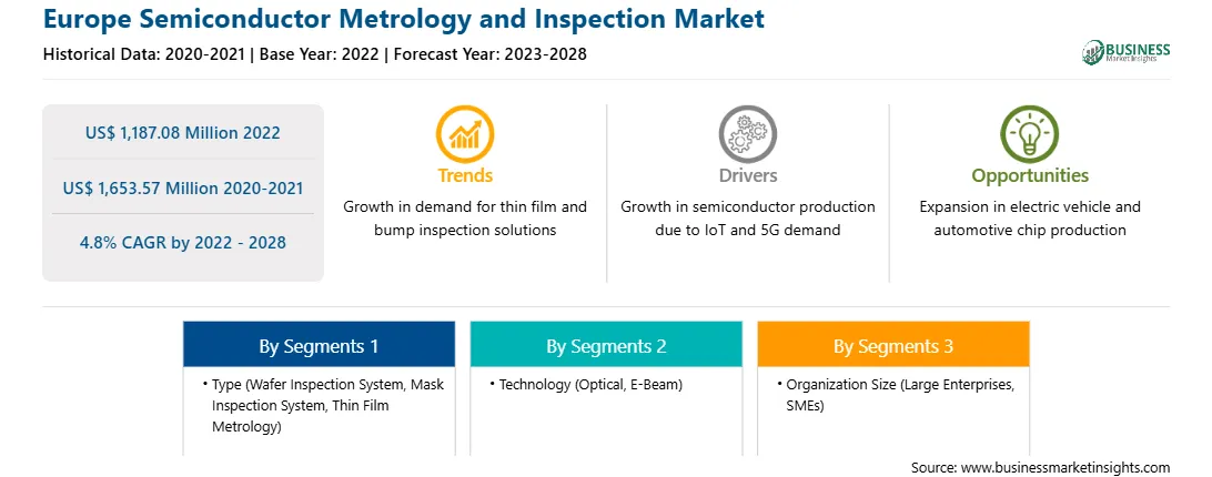
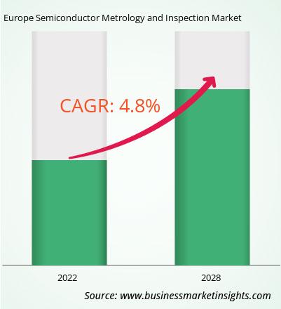
ヨーロッパの半導体計測および検査市場 は、2022 年の 1,187.08 百万米ドルから 1,653.57 米ドル に成長すると予想されています2028 年までに 100 万人。 2022 年から 2028 年にかけて 4.8% の CAGR で成長すると推定されています。
ウェーハの製造、製造、などの手順では、高度なパッケージング (AP) テクノロジーが使用されます。これらの動作をバックエンドで制御するには、検査および測定方法が必要です。フィーチャーサイズの縮小により、高精度、高精度、感度、およびスループットの需要が高まっています。一方、AP 手順は、バンプ計測や非視覚的欠陥など、バックエンド アプリケーションに特有の測定および検査の問題に直面しています。特殊な要件が、AP プロセスの多様性の増加と急速な進化と相まって、2 次元 (2D) および 3 次元 (3D) 形状を含む幅広いパラメータを制御できる柔軟な測定および検査システムの需要を促進しています。新しい要件が発生したときに、それに適応することができます。さまざまなコンピテンシーを 1 つのプラットフォームに統合することが、資本を最も経済的かつ効果的に使用できます。業界のロードマップに対応するには、AP 運用の固有の要件に焦点を当てた機器プロバイダーによる新しいソリューションが必要です。たとえば、KLA Corporation は、3D IC や高密度ファンアウトなどの高度なウェーハレベル パッケージング (AWLP) アプリケーションにおいて、高解像度光学系を備えた Kronos 1190 パターン付きウェーハ検査システムを提供しています。このシステムは、プロセス開発と生産監視のための重要な欠陥に対する感度を提供します。メーカーは品質と信頼性を向上させるというプレッシャーにさらされています。これは、消費者の安全が大きな懸念事項である自動車などの業界に特に当てはまります。自動車には何千もの半導体部品が存在します。さらに、完全な自動運転車では、コンポーネントの数が桁違いに増加する可能性があります。 10,000 個のコンポーネントを備えた自動車の場合、コンポーネントの故障率が 100 万分の 1 であれば、車両の故障率は 100 分の 1 に相当し、これは容認できません。現在および次世代のパッケージでこの課題に対処するには、マイクロメートルレベルまでの欠陥感度と、大量の生データストリームの中で致命的な欠陥を迅速かつ一貫して識別する能力が必要です。ゲージの再現性と再現性 (R&R) の調査が重要になってきています。エンジニアには、生データを有用なプロセス知識に変えるテクノロジーが必要です。電子ビーム技術は先進的なパッケージングにも採用されています。電子は、電子ビーム検査システムのツール内で生成され、ダイの表面に衝突します。電子が散乱して検出器に戻ってくるため、欠陥のあるチップを検出できるようになります。
新しい機能とテクノロジーにより、ベンダーは次のことが可能になります。新たな顧客を引き付け、新興市場での拠点を拡大します。この要因は、ヨーロッパの半導体計測および検査市場を牽引する可能性があります。 ヨーロッパの半導体計測および検査市場は、予測期間中に良好な CAGR で成長すると予想されます。
ヨーロッパの半導体計測および検査市場の収益と 2028 年までの予測 (百万米ドル)
< strong>
ヨーロッパの半導体計測および検査市場のセグメンテーション
ヨーロッパの半導体計測および検査市場は細分化されていますタイプ、テクノロジー、組織の規模、国に基づいて決定されます。ヨーロッパの半導体計測および検査市場は、タイプに基づいて、ウェーハ検査システム、マスク検査システム、薄膜計測に分類されます。 2022 年にはウェーハ検査システム部門が市場を支配しました。ヨーロッパの半導体計測および検査市場は、テクノロジーに基づいて光学と電子ビームに二分されます。 2022 年には光学セグメントが市場を支配しました。組織規模に基づいて、ヨーロッパの半導体計測および検査市場は大企業と中小企業に二分されます。 2022 年の市場は大企業部門が大半を占めました。ヨーロッパの半導体計測および検査市場は、国に基づいて英国、ドイツ、フランス、イタリア、ロシア、およびその他のヨーロッパに分割されています。 2022 年にはドイツが市場を独占しました。
アプライド マテリアルズ株式会社; ASMLホールディングNV;株式会社日立ハイテク、日本電子株式会社; KLAコーポレーション;レーザーテック株式会社;ニコンメトロロジーNV;ノバ株式会社;イノベーションへ。 Thermo Fisher Scientific Inc. と Thermo Fisher Scientific Inc. は、ヨーロッパの半導体計測および検査市場の大手企業の 1 つです。
Strategic insights for Europe Semiconductor Metrology and Inspection involve closely monitoring industry trends, consumer behaviours, and competitor actions to identify opportunities for growth. By leveraging data analytics, businesses can anticipate market shifts and make informed decisions that align with evolving customer needs. Understanding these dynamics helps companies adjust their strategies proactively, enhance customer engagement, and strengthen their competitive edge. Building strong relationships with stakeholders and staying agile in response to changes ensures long-term success in any market.
| Report Attribute | Details |
|---|---|
| Market size in 2022 | US$ 1,187.08 Million |
| Market Size by 2028 | US$ 1,653.57 Million |
| Global CAGR (2022 - 2028) | 4.8% |
| Historical Data | 2020-2021 |
| Forecast period | 2023-2028 |
| Segments Covered |
By タイプ
|
| Regions and Countries Covered | ヨーロッパ
|
| Market leaders and key company profiles |
The regional scope of Europe Semiconductor Metrology and Inspection refers to the geographical area in which a business operates and competes. Understanding regional nuances, such as local consumer preferences, economic conditions, and regulatory environments, is crucial for tailoring strategies to specific markets. Businesses can expand their reach by identifying underserved regions or adapting their offerings to meet regional demands. A clear regional focus allows for more effective resource allocation, targeted marketing, and better positioning against local competitors, ultimately driving growth in those specific areas.
The Europe Semiconductor Metrology and Inspection Market is valued at US$ 1,187.08 Million in 2022, it is projected to reach US$ 1,653.57 Million by 2028.
As per our report Europe Semiconductor Metrology and Inspection Market, the market size is valued at US$ 1,187.08 Million in 2022, projecting it to reach US$ 1,653.57 Million by 2028. This translates to a CAGR of approximately 4.8% during the forecast period.
The Europe Semiconductor Metrology and Inspection Market report typically cover these key segments-
The historic period, base year, and forecast period can vary slightly depending on the specific market research report. However, for the Europe Semiconductor Metrology and Inspection Market report:
The Europe Semiconductor Metrology and Inspection Market is populated by several key players, each contributing to its growth and innovation. Some of the major players include:
The Europe Semiconductor Metrology and Inspection Market report is valuable for diverse stakeholders, including:
Essentially, anyone involved in or considering involvement in the Europe Semiconductor Metrology and Inspection Market value chain can benefit from the information contained in a comprehensive market report.
Office No. 1011, First floor, Farena Corporate Park, Magarpatta-Mundhwa road, Pune - 411028, Maharashtra, India
US:+16467917070
sales@businessmarketinsights.com


 Get Free Sample For Europe Semiconductor Metrology and Inspection Market
