2028年までのアジア太平洋の半導体計測および検査市場予測 – 新型コロナウイルス感染症の影響と地域分析 – タイプ別(ウェーハ検査システム、マスク検査システム、薄膜計測)、技術別(光学式および電子ビーム)、および組織規模 (大企業と中小企業)
No. of Pages: 126 | Report Code: BMIRE00027255 | Category: Electronics and Semiconductor
No. of Pages: 126 | Report Code: BMIRE00027255 | Category: Electronics and Semiconductor
APAC は、半導体産業にとって最も重要な地域の 1 つです。製造と利用の仕組み。半導体工業会 (SIA) によると、APAC は最大の地域半導体市場であり、中国が単一国最大の市場です。半導体計測・検査装置業界では、多くの企業が提携や提携を結んでいます。たとえば、中国のチップ製造ツールメーカーである深セン JT オートメーション イクイップメントは、2021 年 7 月にファーウェイのハイシリコン テクノロジーズ カンパニーと法的拘束力のある 5 年間の契約覚書を締結しました。両社は半導体パッケージング ツールの開発関係を拡大し、この分野を自立させたいと考えています。 -十分かつ規制されている。したがって、この提携により、パッケージング技術における半導体の使用が増加することになります。 APAC の多くの市場関係者が革新的な製品を市場に投入しています。例えば、株式会社日立ハイテクは、2020年11月に高速欠陥検査SEM※1「CR7300」を導入しました。CR7300は、半導体デバイス製造の生産性向上に貢献する新型レビューSEMです。電子光学に基づいており、最高の高解像度画像取得が可能です。同時に、新しいイメージングおよびステージ技術により、従来の方法の半分の時間で高速画像取得が可能となり、総検査時間の大幅な短縮につながります。上記の技術革新により、予測期間中にアジア太平洋地域の半導体計測および検査市場のプレーヤーに機会が生まれると予想されます。
新しい機能とテクノロジーにより、ベンダーは次のことが可能になります。新たな顧客を引き付け、新興市場での拠点を拡大します。この要因は、アジア太平洋地域の半導体計測および検査市場を牽引する可能性があります。 アジア太平洋の半導体計測および検査市場は、予測期間中に良好な CAGR で成長すると予想されます。
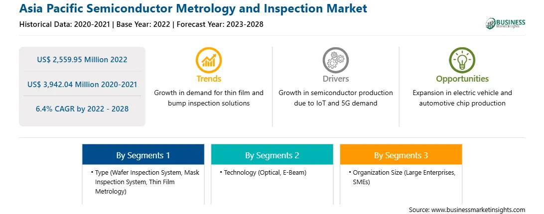
APAC の半導体計測および検査市場は、種類、テクノロジー、組織規模、国に基づいて分割されています。 APACの半導体計測および検査市場は、タイプに基づいて、ウェーハ検査システム、マスク検査システム、薄膜計測に分類されます。 2022 年の市場はウェーハ検査システム部門が独占しました。テクノロジーに基づいて、APAC の半導体計測および検査市場は光学と電子ビームに二分されます。 2022 年には光学セグメントが市場を支配しました。組織規模に基づいて、APAC の半導体計測および検査市場は大企業と中小企業に二分されます。 2022 年の市場は大企業セグメントが大半を占めました。アジア太平洋の半導体計測および検査市場は、国別に中国、インド、日本、韓国、台湾、およびその他のアジア太平洋地域に分割されています。 2022 年には中国が市場を独占しました。
アプライド マテリアルズ株式会社; ASMLホールディングNV;株式会社日立ハイテク、日本電子株式会社; KLAコーポレーション;レーザーテック株式会社;ニコンメトロロジーNV;ノバ株式会社;イノベーションへ。 Thermo Fisher Scientific Inc. は、APAC の半導体計測および検査市場における大手企業の 1 つです。
Strategic insights for Asia Pacific Semiconductor Metrology and Inspection involve closely monitoring industry trends, consumer behaviours, and competitor actions to identify opportunities for growth. By leveraging data analytics, businesses can anticipate market shifts and make informed decisions that align with evolving customer needs. Understanding these dynamics helps companies adjust their strategies proactively, enhance customer engagement, and strengthen their competitive edge. Building strong relationships with stakeholders and staying agile in response to changes ensures long-term success in any market.
| Report Attribute | Details |
|---|---|
| Market size in 2022 | US$ 2,559.95 Million |
| Market Size by 2028 | US$ 3,942.04 Million |
| Global CAGR (2022 - 2028) | 6.4% |
| Historical Data | 2020-2021 |
| Forecast period | 2023-2028 |
| Segments Covered |
By タイプ
|
| Regions and Countries Covered | アジア太平洋
|
| Market leaders and key company profiles |
The regional scope of Asia Pacific Semiconductor Metrology and Inspection refers to the geographical area in which a business operates and competes. Understanding regional nuances, such as local consumer preferences, economic conditions, and regulatory environments, is crucial for tailoring strategies to specific markets. Businesses can expand their reach by identifying underserved regions or adapting their offerings to meet regional demands. A clear regional focus allows for more effective resource allocation, targeted marketing, and better positioning against local competitors, ultimately driving growth in those specific areas.
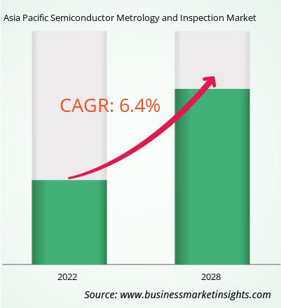
The Asia Pacific Semiconductor Metrology and Inspection Market is valued at US$ 2,559.95 Million in 2022, it is projected to reach US$ 3,942.04 Million by 2028.
As per our report Asia Pacific Semiconductor Metrology and Inspection Market, the market size is valued at US$ 2,559.95 Million in 2022, projecting it to reach US$ 3,942.04 Million by 2028. This translates to a CAGR of approximately 6.4% during the forecast period.
The Asia Pacific Semiconductor Metrology and Inspection Market report typically cover these key segments-
The historic period, base year, and forecast period can vary slightly depending on the specific market research report. However, for the Asia Pacific Semiconductor Metrology and Inspection Market report:
The Asia Pacific Semiconductor Metrology and Inspection Market is populated by several key players, each contributing to its growth and innovation. Some of the major players include:
The Asia Pacific Semiconductor Metrology and Inspection Market report is valuable for diverse stakeholders, including:
Essentially, anyone involved in or considering involvement in the Asia Pacific Semiconductor Metrology and Inspection Market value chain can benefit from the information contained in a comprehensive market report.
Office No. 1011, First floor, Farena Corporate Park, Magarpatta-Mundhwa road, Pune - 411028, Maharashtra, India
US:+16467917070
sales@businessmarketinsights.com


 Get Free Sample For Asia Pacific Semiconductor Metrology and Inspection Market
