Previsioni di mercato dei wafer EPI di silicio per il Nord America fino al 2028 – Impatto del COVID-19 e analisi regionale – Dimensioni del wafer (6 pollici, 8 pollici, 12 pollici e altri), applicazione (LED, semiconduttori di potenza e dispositivi basati su MEMS) ), Utente finale (Elettronica di consumo, Automotive, Sanità, Aerospaziale e difesa e altri) e Tipo (Eteroepitassia e Omoepitassia)
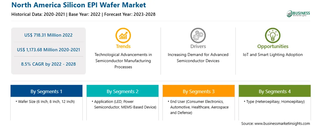
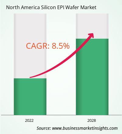
Si prevede che il mercato dei wafer di silicio EPI del Nord America crescerà da 718,31 milioni di dollari nel 2022 a 1.173,68 milioni di dollari entro il 2028; si stima che crescerà a un CAGR del 8,5% dal 2022 al 2028.
Un wafer epitassiale, noto anche come wafer EPI, viene creato posizionando uno strato di silicio monocristallino epitassiale su un wafer di silicio monocristallino . Questo wafer aiuta a regolare i profili di drogaggio difficili da gestire utilizzando tecniche convenzionali come la diffusione e l\'impianto ionico. I wafer epitassiali di silicio sono anche il componente principale utilizzato nella produzione di vari dispositivi a semiconduttore che trovano applicazioni nell\'elettronica di consumo, industriale, militare e spaziale. I wafer vengono utilizzati nei substrati di circuiti integrati (IC) bipolari e semiconduttori a ossido di metallo (MOS). Vengono utilizzati anche negli elementi a diodi e transistor. I wafer epitassiali di silicio vengono utilizzati nei gadget elettrici a risparmio energetico e in altri dispositivi con fonti di alimentazione. Sono utilizzati anche nei LED, nei computer, nei tablet, nei cellulari, nei giroscopi e nelle console di gioco. Epiel, un produttore specializzato di wafer epitassiali in silicio, fornisce servizi epitassiali per l\'industria dei semiconduttori. L\'azienda offre una varietà di wafer epitassiali di silicio personalizzati in dimensioni che vanno da 3\" (76 mm) a 8\" (200 mm) per importanti applicazioni di microelettronica, inclusi dispositivi di potenza discreti, circuiti integrati e sensori. Nel 2020, Qromis, una start-up con sede negli Stati Uniti, ha firmato un accordo di licenza con la giapponese Shin-Etsu Chemical per produrre substrati e wafer epitassiali per elettronica di potenza/RF GaN, dispositivi LED e altri dispositivi. L\'azienda ha già reso disponibili substrati QST pronti per GaN da 6 pollici e 8 pollici e \"modelli\" da 6 pollici e 8 pollici con strati GaN micron da 5 pollici e 10 pollici. Sta sviluppando wafer GaN HEMT EPI da 900 V e 1200 V insieme a wafer GaN HEMT EPI da 200 V e 650 V basati su substrati QST da 6 pollici e 8 pollici per strumenti elettronici. L\'azienda intende inoltre creare un secondo impianto di produzione per substrati QST e wafer epitassiali GaN-on-QST, considerando le proiezioni positive dell\'adozione del GaN dovute alla crescita del mercato dei wafer EPI in silicio.
I fornitori del mercato dei wafer di silicio EPI del Nord America possono attrarre nuovi clienti ed espandere la propria presenza nei mercati emergenti fornendo prodotti innovativi abilitati dalle nuove tecnologie. È probabile che ciò spinga il mercato dei wafer di silicio EPI del Nord America a un CAGR notevole durante il periodo di previsione.
Entrate e previsioni del mercato dei wafer di silicio EPI del Nord America fino al 2028 (milioni di dollari)
Segmentazione del mercato dei wafer di silicio EPI del Nord America
Il mercato dei wafer EPI in silicio del Nord America è segmentato sulla base della dimensione del wafer, dell\'applicazione, dell\'utente finale, del tipo e del paese. In base alle dimensioni del wafer, il mercato è segmentato in 6 pollici, 8 pollici, 12 pollici e altri. In base all\'applicazione, il mercato è suddiviso in dispositivi basati su LED, semiconduttori di potenza e MEMS. In base all\'utente finale, il mercato dei wafer di silicio EPI del Nord America è segmentato in elettronica di consumo, automobilistico, sanitario, aerospaziale e della difesa e altri. In base alla tipologia, il mercato è suddiviso in eteroepitassia e omoepitassia. In base al paese, il mercato dei wafer di silicio EPI del Nord America è segmentato in Stati Uniti, Messico e Canada.
Mercato dei wafer di silicio EPI del Nord America: Aziende menzionate
Materiali applicati, Inc.; II-VI Incorporata; Shin-Etsu Chemical Co., Ltd.; SOCIETÀ SUMCO; Wafer World Inc.; Siltronic AG; NICHIA CORPORATION; EpiGaN nv (Soitec Belgio NV); e SK Siltron Co., Ltd. sono tra le principali aziende che operano nel mercato dei wafer di silicio EPI del Nord America.
North America Silicon EPI Wafer Strategic Insights
Strategic insights for North America Silicon EPI Wafer involve closely monitoring industry trends, consumer behaviours, and competitor actions to identify opportunities for growth. By leveraging data analytics, businesses can anticipate market shifts and make informed decisions that align with evolving customer needs. Understanding these dynamics helps companies adjust their strategies proactively, enhance customer engagement, and strengthen their competitive edge. Building strong relationships with stakeholders and staying agile in response to changes ensures long-term success in any market.
Get more information on this report
North America Silicon EPI Wafer Report Scope
Report Attribute
Details
Market size in 2022
US$ 718.31 Million
Market Size by 2028
US$ 1,173.68 Million
Global CAGR (2022 - 2028)
8.5%
Historical Data
2020-2021
Forecast period
2023-2028
Segments Covered
By Dimensioni del wafer
6 pollici
8 pollici
12 pollici
By Applicazione
LED
semiconduttore di potenza
dispositivo basato su MEMS
By Utente finale
elettronica di consumo
automotive
sanitÃ
aerospaziale e difesa
By Tipo
eteroepitassia
omoepitassia
Regions and Countries Covered
Nord America
Stati Uniti
Canada
Messico
Market leaders and key company profiles
Applied Materials, Inc.
II-VI Incorporated
Shin-Etsu Chemical Co., Ltd.
SUMCO CORPORATION
Wafer World Inc.
Siltronic AG
NICHIA CORPORATION
EpiGaN nv (Soitec Belgium N.V.)
SK Siltron Co., Ltd
Get more information on this report
North America Silicon EPI Wafer Regional Insights
The regional scope of North America Silicon EPI Wafer refers to the geographical area in which a business operates and competes. Understanding regional nuances, such as local consumer preferences, economic conditions, and regulatory environments, is crucial for tailoring strategies to specific markets. Businesses can expand their reach by identifying underserved regions or adapting their offerings to meet regional demands. A clear regional focus allows for more effective resource allocation, targeted marketing, and better positioning against local competitors, ultimately driving growth in those specific areas.
Get more information on this report
Identical Market Reports with other Region/Countries
The List of Companies - North America Silicon EPI Wafer Market
Applied Materials, Inc.
II-VI Incorporated
Shin-Etsu Chemical Co., Ltd.
SUMCO CORPORATION
Wafer World Inc.
Siltronic AG
NICHIA CORPORATION
EpiGaN nv (Soitec Belgium N.V.)
SK Siltron Co., Ltd
Frequently Asked Questions
How big is the North America Silicon EPI Wafer Market?
The North America Silicon EPI Wafer Market is valued at US$ 718.31 Million in 2022, it is projected to reach US$ 1,173.68 Million by 2028.
What is the CAGR for North America Silicon EPI Wafer Market by (2022 - 2028)?
As per our report North America Silicon EPI Wafer Market, the market size is valued at US$ 718.31 Million in 2022, projecting it to reach US$ 1,173.68 Million by 2028. This translates to a CAGR of approximately 8.5% during the forecast period.
What segments are covered in this report?
The North America Silicon EPI Wafer Market report typically cover these key segments-
Dimensioni del wafer (6 pollici, 8 pollici, 12 pollici)
Applicazione (LED, semiconduttore di potenza, dispositivo basato su MEMS)
Utente finale (elettronica di consumo, automotive, sanità, aerospaziale e difesa)
What is the historic period, base year, and forecast period taken for North America Silicon EPI Wafer Market?
The historic period, base year, and forecast period can vary slightly depending on the specific market research report. However, for the North America Silicon EPI Wafer Market report:
Historic Period : 2020-2021
Base Year : 2022
Forecast Period : 2023-2028
Who are the major players in North America Silicon EPI Wafer Market?
The North America Silicon EPI Wafer Market is populated by several key players, each contributing to its growth and innovation. Some of the major players include:
Applied Materials, Inc.
II-VI Incorporated
Shin-Etsu Chemical Co., Ltd.
SUMCO CORPORATION
Wafer World Inc.
Siltronic AG
NICHIA CORPORATION
EpiGaN nv (Soitec Belgium N.V.)
SK Siltron Co., Ltd
Who should buy this report?
The North America Silicon EPI Wafer Market report is valuable for diverse stakeholders, including:
Investors: Provides insights for investment decisions pertaining to market growth, companies, or industry insights. Helps assess market attractiveness and potential returns.
Industry Players: Offers competitive intelligence, market sizing, and trend analysis to inform strategic planning, product development, and sales strategies.
Suppliers and Manufacturers: Helps understand market demand for components, materials, and services related to concerned industry.
Researchers and Consultants: Provides data and analysis for academic research, consulting projects, and market studies.
Financial Institutions: Helps assess risks and opportunities associated with financing or investing in the concerned market.
Essentially, anyone involved in or considering involvement in the North America Silicon EPI Wafer Market value chain can benefit from the information contained in a comprehensive market report.
Get Free Sample For North America Silicon EPI Wafer Market
1. Complete the form
2. Check your inbox (and spam/junk folder)
3. Your Personal Data is Secure with us
GDPR + CCPA Compliant
Personal & transactional information is kept safe from unauthorized use.
WHAT'S INCLUDED IN FULL REPORT : Market Dynamics,
Competitive Analysis and Assessment, Define Business Strategies, Market Outlook and
Trends, Market Size and Share Analysis, Growth Driving Factors, Future Commercial
Potential, Identify Regional Growth Engines


 Get Free Sample For North America Silicon EPI Wafer Market

