Nordamerika-Marktprognose für Silizium-EPI-Wafer bis 2028 – Auswirkungen von COVID-19 und regionale Analyse – Wafergröße (6 Zoll, 8 Zoll, 12 Zoll und andere), Anwendung (LED, Leistungshalbleiter und MEMS-basiertes Gerät). ), Endbenutzer (Unterhaltungselektronik, Automobil, Gesundheitswesen, Luft- und Raumfahrt und Verteidigung und andere) und Typ (Heteroepitaxie und Homoepitaxie)
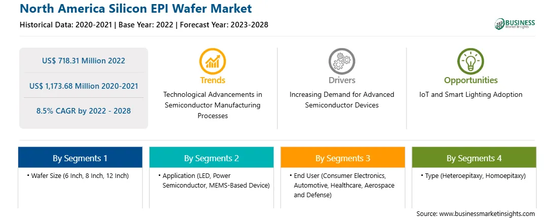
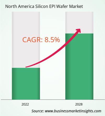
Der nordamerikanische Markt für Silizium-EPI-Wafer wird voraussichtlich von 718,31 Millionen US-Dollar im Jahr 2022 auf 1.173,68 Millionen US-Dollar im Jahr 2028 wachsen; Es wird geschätzt, dass es von 2022 bis 2028 mit einer durchschnittlichen jährlichen Wachstumsrate von 8,5 % wachsen wird.
Ein epitaktischer Wafer, auch EPI-Wafer genannt, entsteht durch die Platzierung einer Schicht epitaktischen Silizium-Einkristalls auf einem einkristallinen Silizium-Wafer . Dieser Wafer hilft bei der Regulierung von Dotierungsprofilen, die mit herkömmlichen Techniken wie Diffusion und Ionenimplantation schwer zu bewältigen sind. Silizium-Epitaxiewafer sind auch die Hauptkomponente, die bei der Herstellung verschiedener Halbleiterbauelemente verwendet wird, die in der Verbraucher-, Industrie-, Militär- und Raumfahrtelektronik Anwendung finden. Die Wafer werden in bipolaren und Metalloxid-Halbleiter (MOS)-Substraten für integrierte Schaltkreise (IC) verwendet. Sie werden auch in Dioden- und Transistorelementen verwendet. Silizium-Epitaxiewafer werden in energiesparenden Geräten und anderen Geräten mit Stromquellen verwendet. Sie werden auch in LEDs, Computern, Tablets, Mobiltelefonen, Gyroskopen und Spielekonsolen verwendet. Epiel, ein spezialisierter Hersteller von Silizium-Epitaxiewafern, bietet Epitaxiedienstleistungen für die Halbleiterindustrie an. Das Unternehmen bietet eine Vielzahl kundenspezifischer epitaktischer Siliziumwafer in Größen von 3 Zoll (76 mm) bis 8 Zoll (200 mm) für wichtige Mikroelektronikanwendungen an, darunter diskrete Leistungsgeräte, integrierte Schaltkreise und Sensoren. Im Jahr 2020 unterzeichnete Qromis, ein in den USA ansässiges Start-up, eine Lizenzvereinbarung mit dem japanischen Unternehmen Shin-Etsu Chemical zur Herstellung von Substraten und epitaktischen Wafern für GaN-Leistungs-/HF-Elektronik, LED-Geräte und andere Geräte. Das Unternehmen hat bereits 6-Zoll- und 8-Zoll-GaN-fähige QST-Substrate sowie 6-Zoll- und 8-Zoll-„Vorlagen“ mit 5-Zoll- und 10-Zoll-Mikrometer-GaN-Schichten bereitgestellt. Es entwickelt 900-V- und 1200-V-GaN-HEMT-EPI-Wafer sowie 200-V- und 650-V-GaN-HEMT-EPI-Wafer auf Basis von 6-Zoll- und 8-Zoll-QST-Substraten für elektronische Instrumente. Das Unternehmen beabsichtigt außerdem, eine zweite Produktionsanlage für QST-Substrate und GaN-auf-QST-Epitaxie-Wafer zu errichten, da die positiven Prognosen für die Einführung von GaN aufgrund des Wachstums des Silizium-EPI-Wafer-Marktes positiv sind.
Anbieter auf dem nordamerikanischen Markt für Silizium-EPI-Wafer können neue Kunden gewinnen und ihre Präsenz in Schwellenmärkten erweitern, indem sie innovative Produkte anbieten, die durch neue Technologien ermöglicht werden. Dies dürfte den nordamerikanischen Markt für Silizium-EPI-Wafer im Prognosezeitraum mit einer bemerkenswerten CAGR ankurbeln.
Umsatz und Prognose für den Markt für Silizium-EPI-Wafer in Nordamerika bis 2028 (Mio. US-Dollar)
Marktsegmentierung für Silizium-EPI-Wafer in Nordamerika
Der nordamerikanische Markt für Silizium-EPI-Wafer ist segmentiert basierend auf Wafergröße, Anwendung, Endbenutzer, Typ und Land. Basierend auf der Wafergröße wird der Markt in 6 Zoll, 8 Zoll, 12 Zoll und andere unterteilt. Je nach Anwendung ist der Markt in LED-, Leistungshalbleiter- und MEMS-basierte Geräte unterteilt. Nach Endverbraucher ist der nordamerikanische Markt für Silizium-EPI-Wafer in Unterhaltungselektronik, Automobil, Gesundheitswesen, Luft- und Raumfahrt und Verteidigung und andere unterteilt. Je nach Typ wird der Markt in Heteroepitaxie und Homoepitaxie unterteilt. Je nach Land ist der nordamerikanische Markt für Silizium-EPI-Wafer in die USA, Mexiko und Kanada unterteilt.
Nordamerikanischer Silizium-EPI-Wafer-Markt – Erwähnte Unternehmen
Applied Materials, Inc.; II-VI Incorporated; Shin-Etsu Chemical Co., Ltd.; SUMCO CORPORATION; Wafer World Inc.; Siltronic AG; NICHIA CORPORATION; EpiGaN nv (Soitec Belgium NV); und SK Siltron Co., Ltd. gehören zu den großen Unternehmen, die auf dem nordamerikanischen Markt für Silizium-EPI-Wafer tätig sind.
North America Silicon EPI Wafer Strategic Insights
Strategic insights for North America Silicon EPI Wafer involve closely monitoring industry trends, consumer behaviours, and competitor actions to identify opportunities for growth. By leveraging data analytics, businesses can anticipate market shifts and make informed decisions that align with evolving customer needs. Understanding these dynamics helps companies adjust their strategies proactively, enhance customer engagement, and strengthen their competitive edge. Building strong relationships with stakeholders and staying agile in response to changes ensures long-term success in any market.
Get more information on this report
North America Silicon EPI Wafer Report Scope
Report Attribute
Details
Market size in 2022
US$ 718.31 Million
Market Size by 2028
US$ 1,173.68 Million
Global CAGR (2022 - 2028)
8.5%
Historical Data
2020-2021
Forecast period
2023-2028
Segments Covered
By Wafergröße
6 Zoll
8 Zoll
12 Zoll
By Anwendung
LED
Leistungshalbleiter
MEMS-basiertes Gerät
By Endbenutzer
Unterhaltungselektronik
Automobil
Gesundheitswesen
Luft- und Raumfahrt und Verteidigung
By Typ
Heteroepitaxie
Homoepitaxie
Regions and Countries Covered
Nordamerika
USA
Kanada
Mexiko
Market leaders and key company profiles
Applied Materials, Inc.
II-VI Incorporated
Shin-Etsu Chemical Co., Ltd.
SUMCO CORPORATION
Wafer World Inc.
Siltronic AG
NICHIA CORPORATION
EpiGaN nv (Soitec Belgium N.V.)
SK Siltron Co., Ltd
Get more information on this report
North America Silicon EPI Wafer Regional Insights
The regional scope of North America Silicon EPI Wafer refers to the geographical area in which a business operates and competes. Understanding regional nuances, such as local consumer preferences, economic conditions, and regulatory environments, is crucial for tailoring strategies to specific markets. Businesses can expand their reach by identifying underserved regions or adapting their offerings to meet regional demands. A clear regional focus allows for more effective resource allocation, targeted marketing, and better positioning against local competitors, ultimately driving growth in those specific areas.
Get more information on this report
Identical Market Reports with other Region/Countries
The List of Companies - North America Silicon EPI Wafer Market
Applied Materials, Inc.
II-VI Incorporated
Shin-Etsu Chemical Co., Ltd.
SUMCO CORPORATION
Wafer World Inc.
Siltronic AG
NICHIA CORPORATION
EpiGaN nv (Soitec Belgium N.V.)
SK Siltron Co., Ltd
Frequently Asked Questions
How big is the North America Silicon EPI Wafer Market?
The North America Silicon EPI Wafer Market is valued at US$ 718.31 Million in 2022, it is projected to reach US$ 1,173.68 Million by 2028.
What is the CAGR for North America Silicon EPI Wafer Market by (2022 - 2028)?
As per our report North America Silicon EPI Wafer Market, the market size is valued at US$ 718.31 Million in 2022, projecting it to reach US$ 1,173.68 Million by 2028. This translates to a CAGR of approximately 8.5% during the forecast period.
What segments are covered in this report?
The North America Silicon EPI Wafer Market report typically cover these key segments-
Endbenutzer (Unterhaltungselektronik, Automobil, Gesundheitswesen, Luft- und Raumfahrt und Verteidigung)
What is the historic period, base year, and forecast period taken for North America Silicon EPI Wafer Market?
The historic period, base year, and forecast period can vary slightly depending on the specific market research report. However, for the North America Silicon EPI Wafer Market report:
Historic Period : 2020-2021
Base Year : 2022
Forecast Period : 2023-2028
Who are the major players in North America Silicon EPI Wafer Market?
The North America Silicon EPI Wafer Market is populated by several key players, each contributing to its growth and innovation. Some of the major players include:
Applied Materials, Inc.
II-VI Incorporated
Shin-Etsu Chemical Co., Ltd.
SUMCO CORPORATION
Wafer World Inc.
Siltronic AG
NICHIA CORPORATION
EpiGaN nv (Soitec Belgium N.V.)
SK Siltron Co., Ltd
Who should buy this report?
The North America Silicon EPI Wafer Market report is valuable for diverse stakeholders, including:
Investors: Provides insights for investment decisions pertaining to market growth, companies, or industry insights. Helps assess market attractiveness and potential returns.
Industry Players: Offers competitive intelligence, market sizing, and trend analysis to inform strategic planning, product development, and sales strategies.
Suppliers and Manufacturers: Helps understand market demand for components, materials, and services related to concerned industry.
Researchers and Consultants: Provides data and analysis for academic research, consulting projects, and market studies.
Financial Institutions: Helps assess risks and opportunities associated with financing or investing in the concerned market.
Essentially, anyone involved in or considering involvement in the North America Silicon EPI Wafer Market value chain can benefit from the information contained in a comprehensive market report.
Get Free Sample For North America Silicon EPI Wafer Market
1. Complete the form
2. Check your inbox (and spam/junk folder)
3. Your Personal Data is Secure with us
GDPR + CCPA Compliant
Personal & transactional information is kept safe from unauthorized use.
WHAT'S INCLUDED IN FULL REPORT : Market Dynamics,
Competitive Analysis and Assessment, Define Business Strategies, Market Outlook and
Trends, Market Size and Share Analysis, Growth Driving Factors, Future Commercial
Potential, Identify Regional Growth Engines


 Get Free Sample For North America Silicon EPI Wafer Market

