Europa-Marktprognose für Halbleitermesstechnik und -inspektion bis 2028 – Auswirkungen von COVID-19 und regionale Analyse – nach Typ (Wafer-Inspektionssystem, Masken-Inspektionssystem und Dünnschichtmesstechnik), Technologie (optisch und E-Beam) und Organisation Größe (Großunternehmen und KMU) Â Â Â
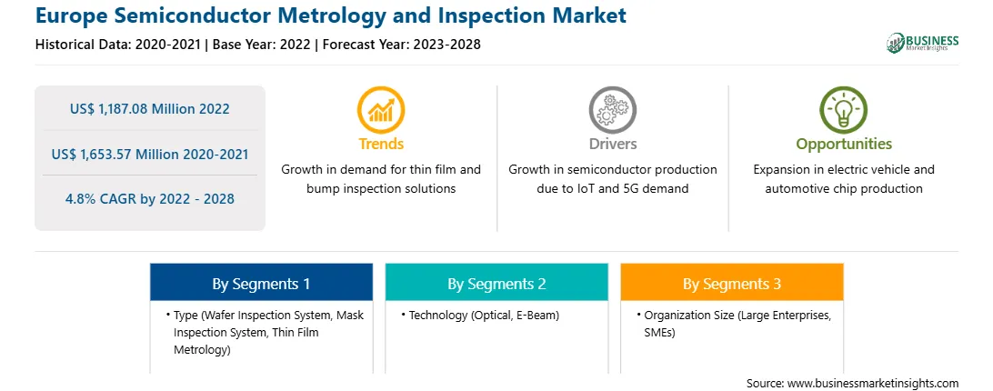
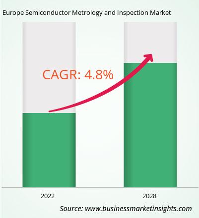
Es wird erwartet, dass der europäische Markt für Halbleitermesstechnik und -inspektion in Europa von 1.187,08 Millionen US-Dollar im Jahr 2022 auf 1.653,57 Millionen US-Dollar wachsen wird /span>Millionen bis 2028; Von 2022 bis 2028 wird ein durchschnittliches jährliches Wachstum von 4,8 % erwartet.
Waferherstellung, Herstellung, und andere Verfahren nutzen die fortschrittliche Verpackungstechnologie (AP). Die Steuerung dieser Vorgänge im Backend erfordert Inspektions- und Messmethoden. Schrumpfende Strukturgrößen steigern die Nachfrage nach hoher Genauigkeit, Präzision, Empfindlichkeit und Durchsatz. Andererseits sind AP-Verfahren mit Mess- und Inspektionsproblemen konfrontiert, wie z. B. Unebenheitsmesstechnik und nicht sichtbaren Fehlern, die nur bei Back-End-Anwendungen auftreten. Besondere Anforderungen in Verbindung mit der zunehmenden Vielfalt und schnellen Entwicklung von AP-Prozessen steigern die Nachfrage nach flexiblen Mess- und Inspektionssystemen, die eine breite Palette von Parametern steuern können, einschließlich zweidimensionaler (2D) und dreidimensionaler (3D) Geometrien können jederzeit an neue Anforderungen angepasst werden. Die Kombination verschiedener Kompetenzen auf einer einzigen Plattform ist der wirtschaftlichste und effektivste Kapitaleinsatz. Um mit der Roadmap der Branche Schritt zu halten, sind neuartige Lösungen von Ausrüstungsanbietern erforderlich, die sich auf die besonderen Anforderungen des AP-Betriebs konzentrieren. Beispielsweise bietet die KLA Corporation das strukturierte Wafer-Inspektionssystem Kronos 1190 mit hochauflösender Optik für Advanced Wafer-Level Packaging (AWLP)-Anwendungen wie 3D-IC und High-Density-Fan-out an. Das System erkennt wichtige Fehler bei der Prozessentwicklung und Produktionsüberwachung. Hersteller stehen unter dem Druck, Qualität und Zuverlässigkeit zu verbessern. Dies gilt insbesondere für Branchen wie die Automobilindustrie, in denen die Sicherheit der Verbraucher ein wichtiges Anliegen ist. In Autos gibt es Tausende von Halbleiterkomponenten. Darüber hinaus könnte sich die Anzahl der Komponenten in völlig autonomen Fahrzeugen um Größenordnungen erhöhen. Bei einem Auto mit 10.000 Bauteilen entspricht eine Bauteilausfallrate von eins zu einer Million einer Fahrzeugausfallrate von einem zu 100, was inakzeptabel ist. Um dieser Herausforderung in aktuellen und nächsten Generationen von Paketen gerecht zu werden, sind eine Fehlerempfindlichkeit bis in den Mikrometerbereich und die Fähigkeit erforderlich, tödliche Fehler schnell und konsistent inmitten riesiger Rohdatenströme zu erkennen. Untersuchungen zur Wiederholbarkeit und Reproduzierbarkeit von Messgeräten (R&R) werden immer relevanter. Ingenieure benötigen Technologien, um Rohdaten in nützliches Prozesswissen umzuwandeln. Die E-Beam-Technologie wird auch in fortschrittlichen Verpackungen eingesetzt. In einem Elektronenstrahl-Inspektionssystem werden im Werkzeug Elektronen erzeugt, die dann auf die Oberfläche eines Stempels treffen. Die Elektronen werden gestreut und zu einem Detektor zurückgeworfen, sodass dieser Chips mit Fehlern erkennen kann.
Mit den neuen Funktionen und Technologien können Anbieter dies tun Gewinnen Sie neue Kunden und erweitern Sie Ihre Präsenz in Schwellenmärkten. Dieser Faktor dürfte den europäischen Markt für Halbleitermesstechnik und -inspektion antreiben. Es wird erwartet, dass der Europa-Markt für Halbleitermesstechnik und -inspektion im Prognosezeitraum mit einer guten jährlichen Wachstumsrate wachsen wird.
Umsatz und Prognose für den Halbleitermess- und Inspektionsmarkt in Europa bis 2028 (Mio. US-Dollar)
< strong>
Europa Marktsegmentierung für Halbleitermesstechnik und -inspektion
Der europäische Markt für Halbleitermesstechnik und -prüfung ist segmentiert basierend auf Typ, Technologie, Organisationsgröße und Land. Je nach Typ ist der europäische Markt für Halbleitermesstechnik und -prüfung in Wafer-Prüfsysteme, Maskenprüfsysteme und Dünnschichtmesstechnik unterteilt. Das Segment der Wafer-Inspektionssysteme dominierte den Markt im Jahr 2022. Basierend auf der Technologie ist der europäische Markt für Halbleitermesstechnik und -inspektion in optische und elektronische Strahlen unterteilt. Das optische Segment dominierte den Markt im Jahr 2022. Basierend auf der Unternehmensgröße ist der europäische Markt für Halbleitermesstechnik und -inspektion in große Unternehmen und KMU unterteilt. Das Segment der Großunternehmen dominierte den Markt im Jahr 2022. Basierend auf dem Land wurde der europäische Markt für Halbleitermesstechnik und -inspektion in Großbritannien, Deutschland, Frankreich, Italien, Russland und das übrige Europa unterteilt. Deutschland dominierte den Markt im Jahr 2022.
Applied Materials, Inc.; ASML Holding NV; Hitachi High-Tech Corporation; JEOL Ltd; KLA Corporation; Lasertec Corporation; Nikon Metrology NV; Nova Ltd.; Auf Innovation; und Thermo Fisher Scientific Inc. gehören zu den führenden Unternehmen auf dem europäischen Markt für Halbleitermesstechnik und -inspektion.
Europe Semiconductor Metrology and Inspection Strategic Insights
Strategic insights for Europe Semiconductor Metrology and Inspection involve closely monitoring industry trends, consumer behaviours, and competitor actions to identify opportunities for growth. By leveraging data analytics, businesses can anticipate market shifts and make informed decisions that align with evolving customer needs. Understanding these dynamics helps companies adjust their strategies proactively, enhance customer engagement, and strengthen their competitive edge. Building strong relationships with stakeholders and staying agile in response to changes ensures long-term success in any market.
Get more information on this report
Europe Semiconductor Metrology and Inspection Report Scope
Report Attribute
Details
Market size in 2022
US$ 1,187.08 Million
Market Size by 2028
US$ 1,653.57 Million
Global CAGR (2022 - 2028)
4.8%
Historical Data
2020-2021
Forecast period
2023-2028
Segments Covered
By Typ
Wafer-Inspektionssystem
Masken-Inspektionssystem
Dünnschicht-Messtechnik
By Technologie
optisch
E-Beam
By Organisationsgröße
GroÃunternehmen
KMU
Regions and Countries Covered
Europa
Großbritannien
Deutschland
Frankreich
Russland
Italien
Rest von Europa
Market leaders and key company profiles
Applied Materials, Inc.
ASML Holding N.V.
Hitachi High-Tech Corporation
JEOL Ltd
KLA Corporation
Lasertec Corporation
Nikon Metrology NV
Nova Ltd.
Onto Innovation
Thermo Fisher Scientific Inc.
Get more information on this report
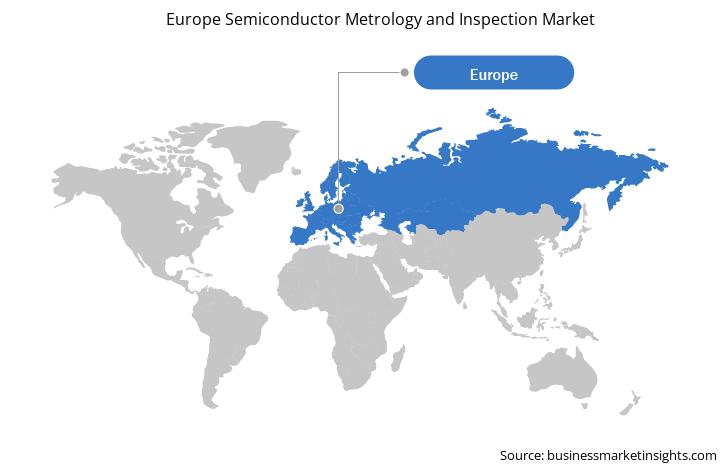
Europe Semiconductor Metrology and Inspection Regional Insights
The regional scope of Europe Semiconductor Metrology and Inspection refers to the geographical area in which a business operates and competes. Understanding regional nuances, such as local consumer preferences, economic conditions, and regulatory environments, is crucial for tailoring strategies to specific markets. Businesses can expand their reach by identifying underserved regions or adapting their offerings to meet regional demands. A clear regional focus allows for more effective resource allocation, targeted marketing, and better positioning against local competitors, ultimately driving growth in those specific areas.
Get more information on this report
Identical Market Reports with other Region/Countries
The List of Companies - Europe Semiconductor Metrology and Inspection Market
Applied Materials, Inc.
ASML Holding N.V.
Hitachi High-Tech Corporation
JEOL Ltd
KLA Corporation
Lasertec Corporation
Nikon Metrology NV
Nova Ltd.
Onto Innovation
Thermo Fisher Scientific Inc.
Frequently Asked Questions
How big is the Europe Semiconductor Metrology and Inspection Market?
The Europe Semiconductor Metrology and Inspection Market is valued at US$ 1,187.08 Million in 2022, it is projected to reach US$ 1,653.57 Million by 2028.
What is the CAGR for Europe Semiconductor Metrology and Inspection Market by (2022 - 2028)?
As per our report Europe Semiconductor Metrology and Inspection Market, the market size is valued at US$ 1,187.08 Million in 2022, projecting it to reach US$ 1,653.57 Million by 2028. This translates to a CAGR of approximately 4.8% during the forecast period.
What segments are covered in this report?
The Europe Semiconductor Metrology and Inspection Market report typically cover these key segments-
Typ (Wafer-Inspektionssystem, Masken-Inspektionssystem, Dünnschicht-Messtechnik)
Technologie (optisch, E-Beam)
Organisationsgröße (Großunternehmen, KMU)
What is the historic period, base year, and forecast period taken for Europe Semiconductor Metrology and Inspection Market?
The historic period, base year, and forecast period can vary slightly depending on the specific market research report. However, for the Europe Semiconductor Metrology and Inspection Market report:
Historic Period : 2020-2021
Base Year : 2022
Forecast Period : 2023-2028
Who are the major players in Europe Semiconductor Metrology and Inspection Market?
The Europe Semiconductor Metrology and Inspection Market is populated by several key players, each contributing to its growth and innovation. Some of the major players include:
Applied Materials, Inc.
ASML Holding N.V.
Hitachi High-Tech Corporation
JEOL Ltd
KLA Corporation
Lasertec Corporation
Nikon Metrology NV
Nova Ltd.
Onto Innovation
Thermo Fisher Scientific Inc.
Who should buy this report?
The Europe Semiconductor Metrology and Inspection Market report is valuable for diverse stakeholders, including:
Investors: Provides insights for investment decisions pertaining to market growth, companies, or industry insights. Helps assess market attractiveness and potential returns.
Industry Players: Offers competitive intelligence, market sizing, and trend analysis to inform strategic planning, product development, and sales strategies.
Suppliers and Manufacturers: Helps understand market demand for components, materials, and services related to concerned industry.
Researchers and Consultants: Provides data and analysis for academic research, consulting projects, and market studies.
Financial Institutions: Helps assess risks and opportunities associated with financing or investing in the concerned market.
Essentially, anyone involved in or considering involvement in the Europe Semiconductor Metrology and Inspection Market value chain can benefit from the information contained in a comprehensive market report.
Get Free Sample For Europe Semiconductor Metrology and Inspection Market
1. Complete the form
2. Check your inbox (and spam/junk folder)
3. Your Personal Data is Secure with us
GDPR + CCPA Compliant
Personal & transactional information is kept safe from unauthorized use.
WHAT'S INCLUDED IN FULL REPORT : Market Dynamics,
Competitive Analysis and Assessment, Define Business Strategies, Market Outlook and
Trends, Market Size and Share Analysis, Growth Driving Factors, Future Commercial
Potential, Identify Regional Growth Engines


 Get Free Sample For Europe Semiconductor Metrology and Inspection Market

