Marktprognose für Halbleitermesstechnik und -inspektion im asiatisch-pazifischen Raum bis 2028 – Auswirkungen von COVID-19 und regionale Analyse – nach Typ (Wafer-Inspektionssystem, Masken-Inspektionssystem und Dünnschichtmesstechnik), Technologie (optisch und E-Beam) und Organisationsgröße (Großunternehmen und KMU) Â Â Â
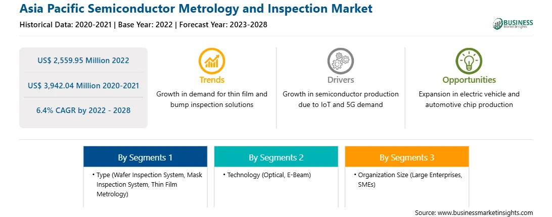
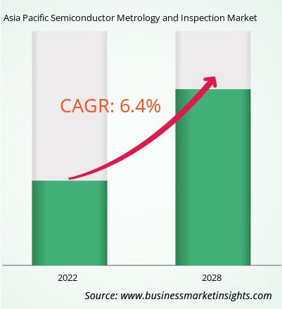
Es wird erwartet, dass der APAC-Markt für Halbleitermesstechnik und -inspektion von 2.559,95 Millionen US-Dollar im Jahr 2022 auf 3.942,04 Millionen US-Dollar wächst Millionen bis 2028; Von 2022 bis 2028 wird ein durchschnittliches jährliches Wachstum von 6,4 % erwartet.
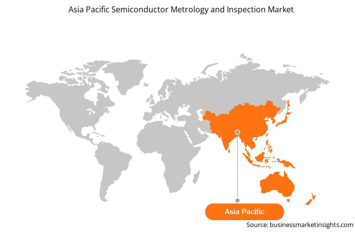
APAC ist eine der wichtigsten Regionen für die Halbleiterindustrie der Herstellung und Nutzung. Nach Angaben der Semiconductor Industry Association (SIA) ist APAC der größte regionale Halbleitermarkt, wobei China der größte Einzellandmarkt ist. Viele Unternehmen bilden Allianzen und Partnerschaften in der Halbleitermess-/Inspektionsgeräteindustrie. Beispielsweise hat Shenzhen JT Automation Equipment, ein chinesischer Hersteller von Chip-Fertigungswerkzeugen, im Juli 2021 eine rechtsverbindliche fünfjährige Vereinbarung mit Huaweis HiSilicon Technologies Company geschlossen. Beide Unternehmen wollen ihre Beziehung zur Entwicklung von Halbleiter-Verpackungswerkzeugen ausbauen und den Sektor unabhängig machen -ausreichend und reguliert. Somit wird die Partnerschaft den Einsatz von Halbleitern in der Verpackungstechnologie steigern. Viele Marktteilnehmer in APAC bringen innovative Produkte auf den Markt. Beispielsweise hat Hitachi High-Tech Corporation im November 2020 die Hochgeschwindigkeits-Fehlerprüfung SEM*1 CR7300 eingeführt. Der CR7300 ist ein neuer Test-REM-Typ, der dazu beitragen wird, die Produktivität bei der Herstellung von Halbleiterbauelementen zu steigern. Es basiert auf Elektronenoptik, was eine beste hochauflösende Bildaufnahme ermöglicht. Gleichzeitig ermöglichen neue Bildgebungs- und Bühnentechnologien eine Hochgeschwindigkeits-Bildaufnahme in der Hälfte der Zeit herkömmlicher Methoden, was zu einer erheblichen Reduzierung der gesamten Inspektionszeit führt. Es wird erwartet, dass die oben genannten technologischen Innovationen im Prognosezeitraum Chancen für Marktteilnehmer im Bereich Halbleitermesstechnik und -prüfung in APAC schaffen.
Mit den neuen Funktionen und Technologien können Anbieter dies tun Gewinnen Sie neue Kunden und erweitern Sie Ihre Präsenz in Schwellenmärkten. Dieser Faktor dürfte den APAC-Markt für Halbleitermesstechnik und -prüfung antreiben. Es wird erwartet, dass der APAC-Markt für Halbleitermesstechnik und -prüfung im Prognosezeitraum mit einer guten jährlichen Wachstumsrate wachsen wird.
Umsatz und Prognose des APAC-Marktes für Halbleitermesstechnik und -inspektion bis 2028 (Mio. US-Dollar)
APAC Semiconductor Metrology and Inspection Marktsegmentierung
Der APAC-Markt für Halbleitermesstechnik und -prüfung ist nach Typ, Technologie, Unternehmensgröße und Land segmentiert. Je nach Typ ist der APAC-Markt für Halbleitermesstechnik und -prüfung in Wafer-Prüfsysteme, Maskenprüfsysteme und Dünnschichtmesstechnik unterteilt. Das Segment der Wafer-Inspektionssysteme dominierte den Markt im Jahr 2022. Basierend auf der Technologie ist der APAC-Markt für Halbleitermesstechnik und -inspektion in optische und elektronische Strahlen unterteilt. Das optische Segment dominierte den Markt im Jahr 2022. Basierend auf der Unternehmensgröße ist der APAC-Markt für Halbleitermesstechnik und -prüfung in große Unternehmen und KMU unterteilt. Das Segment der Großunternehmen dominierte den Markt im Jahr 2022. Basierend auf dem Land wurde der APAC-Markt für Halbleitermesstechnik und -prüfung in China, Indien, Japan, Südkorea, Taiwan und den Rest von APAC segmentiert. China dominierte den Markt im Jahr 2022.
Applied Materials, Inc.; ASML Holding NV; Hitachi High-Tech Corporation; JEOL Ltd; KLA Corporation; Lasertec Corporation; Nikon Metrology NV; Nova Ltd.; Auf Innovation; und Thermo Fisher Scientific Inc. gehören zu den führenden Unternehmen auf dem APAC-Markt für Halbleitermesstechnik und -inspektion.
Asia Pacific Semiconductor Metrology and Inspection Strategic Insights
Strategic insights for Asia Pacific Semiconductor Metrology and Inspection involve closely monitoring industry trends, consumer behaviours, and competitor actions to identify opportunities for growth. By leveraging data analytics, businesses can anticipate market shifts and make informed decisions that align with evolving customer needs. Understanding these dynamics helps companies adjust their strategies proactively, enhance customer engagement, and strengthen their competitive edge. Building strong relationships with stakeholders and staying agile in response to changes ensures long-term success in any market.
Get more information on this report
Asia Pacific Semiconductor Metrology and Inspection Report Scope
Report Attribute
Details
Market size in 2022
US$ 2,559.95 Million
Market Size by 2028
US$ 3,942.04 Million
Global CAGR (2022 - 2028)
6.4%
Historical Data
2020-2021
Forecast period
2023-2028
Segments Covered
By Typ
Wafer-Inspektionssystem
Masken-Inspektionssystem
Dünnschicht-Messtechnik
By Technologie
optisch
E-Beam
By Organisationsgröße
GroÃunternehmen
KMU
Regions and Countries Covered
Asien-Pazifik
China
Indien
Japan
Australien
Rest des Asien-Pazifik-Raums
Market leaders and key company profiles
Applied Materials, Inc.
ASML Holding N.V.
Hitachi High-Tech Corporation
JEOL Ltd
KLA Corporation
Lasertec Corporation
Nikon Metrology NV
Nova Ltd.
Onto Innovation
Thermo Fisher Scientific Inc.
Get more information on this report
Asia Pacific Semiconductor Metrology and Inspection Regional Insights
The regional scope of Asia Pacific Semiconductor Metrology and Inspection refers to the geographical area in which a business operates and competes. Understanding regional nuances, such as local consumer preferences, economic conditions, and regulatory environments, is crucial for tailoring strategies to specific markets. Businesses can expand their reach by identifying underserved regions or adapting their offerings to meet regional demands. A clear regional focus allows for more effective resource allocation, targeted marketing, and better positioning against local competitors, ultimately driving growth in those specific areas.
Get more information on this report
Identical Market Reports with other Region/Countries
The List of Companies - Asia Pacific Semiconductor Metrology and Inspection Market
Applied Materials, Inc.
ASML Holding N.V.
Hitachi High-Tech Corporation
JEOL Ltd
KLA Corporation
Lasertec Corporation
Nikon Metrology NV
Nova Ltd.
Onto Innovation
Thermo Fisher Scientific Inc.
Frequently Asked Questions
How big is the Asia Pacific Semiconductor Metrology and Inspection Market?
The Asia Pacific Semiconductor Metrology and Inspection Market is valued at US$ 2,559.95 Million in 2022, it is projected to reach US$ 3,942.04 Million by 2028.
What is the CAGR for Asia Pacific Semiconductor Metrology and Inspection Market by (2022 - 2028)?
As per our report Asia Pacific Semiconductor Metrology and Inspection Market, the market size is valued at US$ 2,559.95 Million in 2022, projecting it to reach US$ 3,942.04 Million by 2028. This translates to a CAGR of approximately 6.4% during the forecast period.
What segments are covered in this report?
The Asia Pacific Semiconductor Metrology and Inspection Market report typically cover these key segments-
Typ (Wafer-Inspektionssystem, Masken-Inspektionssystem, Dünnschicht-Messtechnik)
Technologie (optisch, E-Beam)
Organisationsgröße (Großunternehmen, KMU)
What is the historic period, base year, and forecast period taken for Asia Pacific Semiconductor Metrology and Inspection Market?
The historic period, base year, and forecast period can vary slightly depending on the specific market research report. However, for the Asia Pacific Semiconductor Metrology and Inspection Market report:
Historic Period : 2020-2021
Base Year : 2022
Forecast Period : 2023-2028
Who are the major players in Asia Pacific Semiconductor Metrology and Inspection Market?
The Asia Pacific Semiconductor Metrology and Inspection Market is populated by several key players, each contributing to its growth and innovation. Some of the major players include:
Applied Materials, Inc.
ASML Holding N.V.
Hitachi High-Tech Corporation
JEOL Ltd
KLA Corporation
Lasertec Corporation
Nikon Metrology NV
Nova Ltd.
Onto Innovation
Thermo Fisher Scientific Inc.
Who should buy this report?
The Asia Pacific Semiconductor Metrology and Inspection Market report is valuable for diverse stakeholders, including:
Investors: Provides insights for investment decisions pertaining to market growth, companies, or industry insights. Helps assess market attractiveness and potential returns.
Industry Players: Offers competitive intelligence, market sizing, and trend analysis to inform strategic planning, product development, and sales strategies.
Suppliers and Manufacturers: Helps understand market demand for components, materials, and services related to concerned industry.
Researchers and Consultants: Provides data and analysis for academic research, consulting projects, and market studies.
Financial Institutions: Helps assess risks and opportunities associated with financing or investing in the concerned market.
Essentially, anyone involved in or considering involvement in the Asia Pacific Semiconductor Metrology and Inspection Market value chain can benefit from the information contained in a comprehensive market report.
Get Free Sample For Asia Pacific Semiconductor Metrology and Inspection Market
1. Complete the form
2. Check your inbox (and spam/junk folder)
3. Your Personal Data is Secure with us
GDPR + CCPA Compliant
Personal & transactional information is kept safe from unauthorized use.
WHAT'S INCLUDED IN FULL REPORT : Market Dynamics,
Competitive Analysis and Assessment, Define Business Strategies, Market Outlook and
Trends, Market Size and Share Analysis, Growth Driving Factors, Future Commercial
Potential, Identify Regional Growth Engines


 Get Free Sample For Asia Pacific Semiconductor Metrology and Inspection Market

