توقعات سوق قياس وفحص أشباه الموصلات في أوروبا حتى عام 2028 – تأثير فيروس كورونا (COVID-19) والتحليل الإقليمي – حسب النوع (نظام فحص الرقاقات، ونظام فحص القناع، ومقاييس الأغشية الرقيقة)، والتكنولوجيا (البصرية والشعاع الإلكتروني)، والتنظيم الحجم (الشركات الكبيرة والشركات الصغيرة والمتوسطة).
– حسب النوع (نظام فحص الرقاقات، ونظام فحص القناع، ومقاييس الأغشية الرقيقة)، والتكنولوجيا (البصرية والشعاع الإلكتروني)، والتنظيم الحجم (الشركات الكبيرة والشركات الصغيرة والمتوسطة).
No. of Pages:
125
|
Report Code:
BMIRE00027261
|
Category:
Electronics and Semiconductor
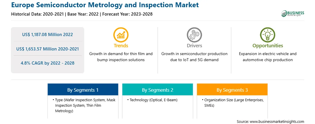
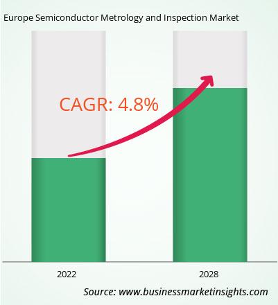
من المتوقع أن ينمو سوق قياس وفحص أشباه الموصلات في أوروبا من 1,187.08 مليون دولار أمريكي في عام 2022 إلى 1,653.57 < /span> مليون بحلول عام 2028؛ ومن المتوقع أن تنمو بمعدل نمو سنوي مركب قدره 4.8% من عام 2022 إلى عام 2028.
تصنيع وتصنيع وتصنيع الرقاقات وتستخدم الإجراءات الأخرى تقنية التغليف المتقدمة (AP). يتطلب التحكم في هذه العمليات في النهاية الخلفية طرق الفحص والقياس. يؤدي تقلص أحجام الميزات إلى زيادة الطلب على الدقة العالية والدقة والحساسية والإنتاجية. من ناحية أخرى، تواجه إجراءات AP مشكلات القياس والفحص، مثل قياس الارتطام والعيوب غير المرئية، التي تنفرد بها التطبيقات الخلفية. المتطلبات الخاصة، جنبًا إلى جنب مع التنوع المتزايد والتطور السريع لعمليات AP، تدفع الطلب على أنظمة القياس والتفتيش المرنة التي يمكنها التحكم في مجموعة واسعة من المعلمات، بما في ذلك الأشكال الهندسية ثنائية الأبعاد (2D) وثلاثية الأبعاد (3D)، و يمكن تكييفها مع المتطلبات الجديدة عند ظهورها. إن الجمع بين مختلف الكفاءات في منصة واحدة هو الاستخدام الأكثر اقتصادا وفعالية لرأس المال. تتطلب مواكبة خريطة طريق الصناعة حلولاً جديدة من موفري المعدات التي تركز على المتطلبات الفريدة لعمليات AP. على سبيل المثال، تقدم شركة KLA نظام Kronos 1190 لفحص الرقائق المزخرفة مع بصريات عالية الدقة في تطبيقات التعبئة والتغليف المتقدمة على مستوى الرقاقة (AWLP) مثل 3D IC والمروحة عالية الكثافة. يعطي النظام حساسية للعيوب الهامة لتطوير العمليات ومراقبة الإنتاج. يتعرض المصنعون لضغوط لتحسين الجودة والاعتمادية. وينطبق هذا بشكل خاص على صناعات مثل السيارات، حيث تشكل سلامة المستهلك مصدر قلق كبير. توجد الآلاف من مكونات أشباه الموصلات في السيارات. بالإضافة إلى ذلك، قد يزيد عدد المكونات بشكل كبير في المركبات ذاتية القيادة تمامًا. بالنسبة لسيارة تحتوي على 10000 مكون، فإن معدل عطل مكون واحد في المليون يعادل معدل عطل السيارة واحد في 100، وهو أمر غير مقبول. ولمواجهة هذا التحدي في حزم الجيل الحالي والقادم، يلزم وجود حساسية للعيوب وصولاً إلى مستوى الميكرومتر والقدرة على تمييز الأخطاء القاتلة بسرعة وباستمرار وسط تدفقات ضخمة من البيانات الأولية. أصبحت تحقيقات قياس التكرار والتكاثر (R&R) ذات صلة. يحتاج المهندسون إلى تقنيات لتحويل البيانات الأولية إلى معرفة عملية مفيدة. كما يتم اعتماد تقنية الشعاع الإلكتروني في العبوات المتقدمة. يتم إنشاء الإلكترونات داخل الأداة في نظام فحص الشعاع الإلكتروني ثم تصطدم بسطح القالب. وتتناثر الإلكترونات وترتد مرة أخرى إلى الكاشف، مما يسمح له باكتشاف الرقائق التي بها عيوب.
بفضل الميزات والتقنيات الجديدة، يمكن للبائعين جذب عملاء جدد وتوسيع نطاق أعمالهم في الأسواق الناشئة. ومن المرجح أن يقود هذا العامل سوق قياس وفحص أشباه الموصلات في أوروبا. من المتوقع أن ينمو سوق قياس وفحص أشباه الموصلات في أوروبا بمعدل نمو سنوي مركب جيد خلال الفترة المتوقعة.
إيرادات وتوقعات سوق قياس أشباه الموصلات والتفتيش في أوروبا حتى عام 2028 (مليون دولار أمريكي)
< قوي>
تجزئة سوق قياس وفحص أشباه الموصلات في أوروبا &نبسب;&نبسب;
سوق قياس وفحص أشباه الموصلات في أوروبا مجزأ بناءً على النوع والتكنولوجيا وحجم المنظمة والبلد. استنادًا إلى النوع، يتم تقسيم سوق قياس وفحص أشباه الموصلات في أوروبا إلى نظام فحص الرقائق ونظام فحص القناع ومقاييس الأغشية الرقيقة. سيطر قطاع أنظمة فحص الرقائق على السوق في عام 2022. واستنادًا إلى التكنولوجيا، ينقسم سوق قياس وفحص أشباه الموصلات في أوروبا إلى شعاع بصري وإلكتروني. سيطر قطاع البصريات على السوق في عام 2022. واستنادًا إلى حجم المنظمة، ينقسم سوق قياس وفحص أشباه الموصلات في أوروبا إلى مؤسسات كبيرة وشركات صغيرة ومتوسطة. سيطر قطاع الشركات الكبيرة على السوق في عام 2022. استنادًا إلى البلد، تم تقسيم سوق قياس وفحص أشباه الموصلات في أوروبا إلى المملكة المتحدة وألمانيا وفرنسا وإيطاليا وروسيا وبقية أوروبا. سيطرت ألمانيا على السوق في عام 2022.
شركة المواد التطبيقية; ASML القابضة NV؛ شركة هيتاشي للتكنولوجيا الفائقة؛ جيول المحدودة؛ شركة جيش تحرير كوسوفو؛ شركة لاسيرتيك؛ نيكون مترولوجي إن في؛ نوفا المحدودة. على الابتكار؛ وشركة Thermo Fisher Scientific Inc. هي من بين الشركات الرائدة في سوق قياس وفحص أشباه الموصلات في أوروبا.
Europe Semiconductor Metrology and Inspection Strategic Insights
Strategic insights for Europe Semiconductor Metrology and Inspection involve closely monitoring industry trends, consumer behaviours, and competitor actions to identify opportunities for growth. By leveraging data analytics, businesses can anticipate market shifts and make informed decisions that align with evolving customer needs. Understanding these dynamics helps companies adjust their strategies proactively, enhance customer engagement, and strengthen their competitive edge. Building strong relationships with stakeholders and staying agile in response to changes ensures long-term success in any market.
Get more information on this report
Europe Semiconductor Metrology and Inspection Report Scope
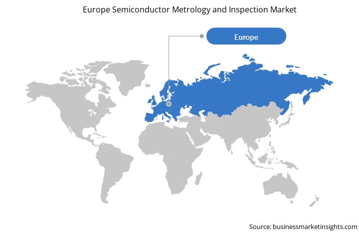
المملكة المتحدة، ألمانيا، فرنسا، روسيا، إيطاليا، بقية أوروبا
Market leaders and key company profiles
Applied Materials, Inc.
ASML Holding N.V.
Hitachi High-Tech Corporation
JEOL Ltd
KLA Corporation
Lasertec Corporation
Nikon Metrology NV
Nova Ltd.
Onto Innovation
Thermo Fisher Scientific Inc.
Get more information on this report
Europe Semiconductor Metrology and Inspection Regional Insights
The regional scope of Europe Semiconductor Metrology and Inspection refers to the geographical area in which a business operates and competes. Understanding regional nuances, such as local consumer preferences, economic conditions, and regulatory environments, is crucial for tailoring strategies to specific markets. Businesses can expand their reach by identifying underserved regions or adapting their offerings to meet regional demands. A clear regional focus allows for more effective resource allocation, targeted marketing, and better positioning against local competitors, ultimately driving growth in those specific areas.
Get more information on this report
Identical Market Reports with other Region/Countries
The List of Companies - Europe Semiconductor Metrology and Inspection Market
Applied Materials, Inc.
ASML Holding N.V.
Hitachi High-Tech Corporation
JEOL Ltd
KLA Corporation
Lasertec Corporation
Nikon Metrology NV
Nova Ltd.
Onto Innovation
Thermo Fisher Scientific Inc.
Frequently Asked Questions
How big is the Europe Semiconductor Metrology and Inspection Market?
The Europe Semiconductor Metrology and Inspection Market is valued at US$ 1,187.08 Million in 2022, it is projected to reach US$ 1,653.57 Million by 2028.
What is the CAGR for Europe Semiconductor Metrology and Inspection Market by (2022 - 2028)?
As per our report Europe Semiconductor Metrology and Inspection Market, the market size is valued at US$ 1,187.08 Million in 2022, projecting it to reach US$ 1,653.57 Million by 2028. This translates to a CAGR of approximately 4.8% during the forecast period.
What segments are covered in this report?
The Europe Semiconductor Metrology and Inspection Market report typically cover these key segments-
النوع (نظام فحص الرقاقة، نظام فحص القناع، قياس الأغشية الرقيقة)
التكنولوجيا (البصرية، الشعاع الإلكتروني)
حجم المنظمة (المؤسسات الكبيرة، الشركات الصغيرة والمتوسطة)
What is the historic period, base year, and forecast period taken for Europe Semiconductor Metrology and Inspection Market?
The historic period, base year, and forecast period can vary slightly depending on the specific market research report. However, for the Europe Semiconductor Metrology and Inspection Market report:
Historic Period : 2020-2021
Base Year : 2022
Forecast Period : 2023-2028
Who are the major players in Europe Semiconductor Metrology and Inspection Market?
The Europe Semiconductor Metrology and Inspection Market is populated by several key players, each contributing to its growth and innovation. Some of the major players include:
Applied Materials, Inc.
ASML Holding N.V.
Hitachi High-Tech Corporation
JEOL Ltd
KLA Corporation
Lasertec Corporation
Nikon Metrology NV
Nova Ltd.
Onto Innovation
Thermo Fisher Scientific Inc.
Who should buy this report?
The Europe Semiconductor Metrology and Inspection Market report is valuable for diverse stakeholders, including:
Investors: Provides insights for investment decisions pertaining to market growth, companies, or industry insights. Helps assess market attractiveness and potential returns.
Industry Players: Offers competitive intelligence, market sizing, and trend analysis to inform strategic planning, product development, and sales strategies.
Suppliers and Manufacturers: Helps understand market demand for components, materials, and services related to concerned industry.
Researchers and Consultants: Provides data and analysis for academic research, consulting projects, and market studies.
Financial Institutions: Helps assess risks and opportunities associated with financing or investing in the concerned market.
Essentially, anyone involved in or considering involvement in the Europe Semiconductor Metrology and Inspection Market value chain can benefit from the information contained in a comprehensive market report.
Get Free Sample For Europe Semiconductor Metrology and Inspection Market
1. Complete the form
2. Check your inbox (and spam/junk folder)
3. Your Personal Data is Secure with us
GDPR + CCPA Compliant
Personal & transactional information is kept safe from unauthorized use.
WHAT'S INCLUDED IN FULL REPORT : Market Dynamics,
Competitive Analysis and Assessment, Define Business Strategies, Market Outlook and
Trends, Market Size and Share Analysis, Growth Driving Factors, Future Commercial
Potential, Identify Regional Growth Engines


 Get Free Sample For Europe Semiconductor Metrology and Inspection Market

